Wiring structure in bending area and display device having same

a display device and wire structure technology, applied in the field of display technology, can solve the problems of poor anti-bend properties of metal wiring in the bending area, affecting the driving of display panels, and not helping in fulfilling the design of “full screen” and other problems, to achieve the effect of ensuring the anti-bend properties of the bending area of display devices and ensuring the stability of signals

Active Publication Date: 2020-10-20
WUHAN CHINA STAR OPTOELECTRONICS SEMICON DISPLAY TECH CO LTD
View PDF10 Cites 1 Cited by
  • Summary
  • Abstract
  • Description
  • Claims
  • Application Information

AI Technical Summary

Benefits of technology

[0034]The present disclosure is characterized by replacing one single signal line with a plurality of signal lines parallel to each other, wherein lateral connection portions are formed between any two adjacent signal lines, and the signal lines are connected to each other at both ends thereof. Therefore, the signals can be transmitted among the signal lines in a same signal line unit, and merge at ends of the signal line unit, thus ensuring delivery stability of signals. In addition, organic protection layers are disposed above and below the signal lines to protect the metal layer where the signal lines are disposed, thus ensuring anti-bend properties of the bending area of display devices.

Problems solved by technology

This does not help in fulfilling “full screen” designs.
However, this requires wiring structures in the bending area to have excellent anti-bend properties; otherwise, the wiring structures will rupture and a malfunction will occur during bending process, affecting driving of display panels.
In summary, because in conventional flexible display devices, metal wirings in the bending area have poor anti-bend properties and are liable to rupture, there is a need to provide a wiring structure in the bending area of flexible display devices in order to solve problems existing in prior art.

Method used


Image

  • Wiring structure in bending area and display device having same
  • Wiring structure in bending area and display device having same
  • Wiring structure in bending area and display device having same

Examples


embodiment one

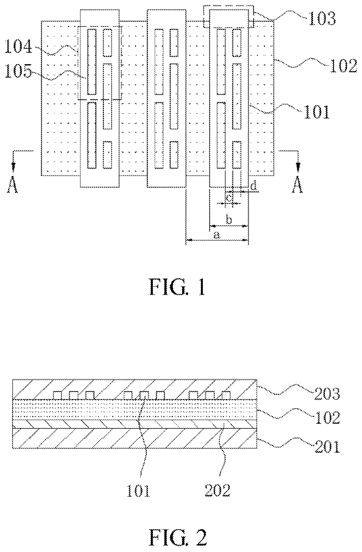
[0044]The present embodiment provides a wiring structure in a bending area. Description thereof is provided below with reference to FIGS. 1 and 2.

[0045]FIG. 1 shows a top view of a wiring structure in a bending area according to the present embodiment. The wiring structure includes a first metal layer 101 and a first organic protection layer 102. The first metal layer 101 is disposed on the first organic protection layer 102. The first metal layer 101 includes a plurality of signal line units 104 spaced apart from each other, wherein each of the signal line units 104 includes at least two signal lines parallel to each other.

[0046]In the present embodiment, each of the signal line units 104 is composed of three signal lines 105. Any two adjacent signal lines 105 are connected to each other by lateral connection portions perpendicular to an extending direction of the signal lines. Any two adjacent connection portions for connecting two adjacent signal lines are positioned to have a st...

embodiment two

[0051]The present embodiment provides a wiring structure in a bending area. Description thereof is provided below with reference to FIGS. 3-6.

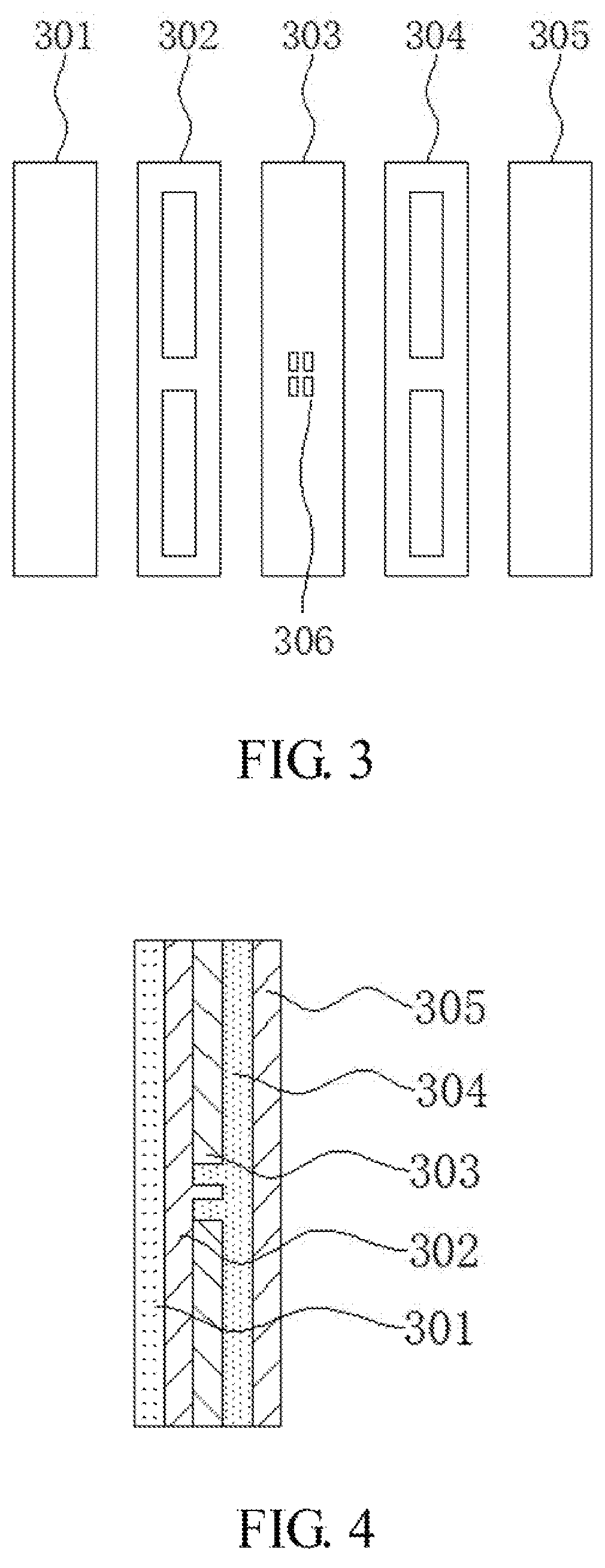
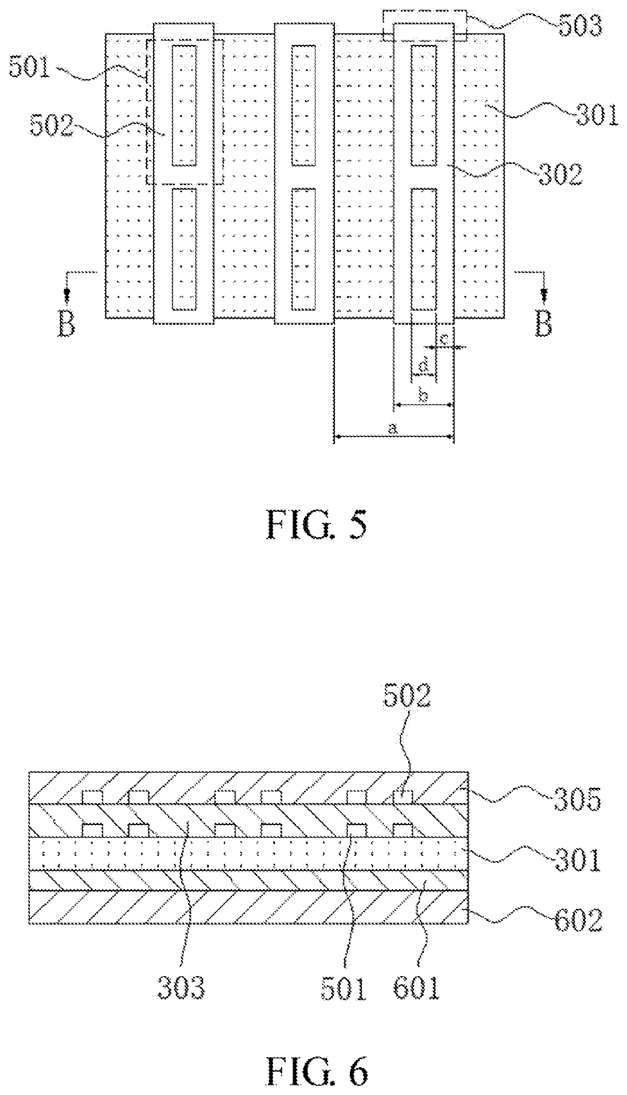
[0052]The present embodiment provides a wiring structure in a bending area. As shown in FIG. 3, the wiring structure includes a first organic protection layer 301, a first metal layer 302, a third organic protection layer 303, a second metal layer 304, and a second organic protection layer 305. The third organic protection layer 303 includes through-holes 306 formed therein.

[0053]Please refer to FIG. 4, which shows a cross-sectional view of the wiring structure taken along a wiring extending direction according to a second structural design. The first metal layer 302 is disposed on the first organic protection layer 301. The third organic protection layer 303 is sandwiched between the first metal layer 302 and the second metal layer 304. The first metal layer 302 and the second metal layer 304 are connected to each other via the through-holes ...

embodiment three

[0058]The present embodiment provides a display device. Description thereof is provided below with reference to FIGS. 1 and 2.

[0059]FIG. 1 shows a top view of a wiring structure in a bending area, where the wiring structure is included in a display device according to the present embodiment. The wiring structure includes a first metal layer 101 and a first organic protection layer 102. The first metal layer 101 is disposed on the first organic protection layer 102. The first metal layer 101 includes a plurality of signal line units 104 spaced apart from each other, wherein each of the signal line units 104 includes at least two signal lines parallel to each other.

[0060]In the present embodiment, each of the signal line units 104 is composed of three signal lines 105. Any two adjacent signal lines 105 are connected to each other by lateral connection portions perpendicular to an extending direction of the signal lines. Any two adjacent connection portions for connecting two adjacent ...


PUM

PropertyMeasurementUnit
bending areaaaaaaaaaaa
widthaaaaaaaaaa
weightaaaaaaaaaa

Abstract

The present disclosure provides a wiring structure in a bending area and a display device having same. The wiring structure includes a substrate, a first organic protection layer, a first metal layer, and a second organic protection layer. The first metal layer is disposed on the first organic protection layer. The second organic protection layer is disposed on the first metal layer, and fills a gap between the signal lines.

Description

FIELD OF INVENTION[0001]The present disclosure relates to a field of display technology, and more particularly to a wiring structure in a bending area and a display panel having same.BACKGROUND[0002]Because organic light emitting display (OLED) display devices are light in weight, flexible, and portable, OLED display devices attract users' attention. OLED display devices with “full screen” designs have become mainstream in recent years, and display panels are thus required to have narrower edge frames. However, edge frames at a bottom side of panels have a greater width than the other three sides of panels because of integrated circuits (ICs) and flexible print circuits (FPCs) disposed therein. This does not help in fulfilling “full screen” designs.[0003]For this reason, flexible OLED display devices nowadays include a bending area in order to have an area outside of the bending area (where fan-out electrical lines, ICs, FPCs, and etc. are disposed) being bent to a backside of panel...

Claims


Application Information

Patent Timeline
Patent Type & Authority Patents(United States)
IPC IPC(8): G09G3/30H01L51/00H01L51/52H01L27/32
CPCH01L51/0097H01L27/3276H01L51/5237G09F9/301G09G3/3208G09G2300/04H10K59/131Y02E10/549H10K59/179H10K77/111H10K50/844H10K2102/311H10K50/84
Inventor LI, XUE
Owner WUHAN CHINA STAR OPTOELECTRONICS SEMICON DISPLAY TECH CO LTD
Why Eureka
Try Eureka