Supercharge Your Innovation With Domain-Expert AI Agents!

Optical package and method of producing an optical package

a technology of optical package and optical package, which is applied in the direction of instruments, lenses, radio frequency control devices, etc., can solve the problems of blocking crosstalk, infrared light, and interfering filters that have progressively larger wavelength shifts in their spectral response curves, so as to improve sensitivity, less prone to optical crosstalk, and easy to handle

Active Publication Date: 2020-11-24
AMS AG
View PDF13 Cites 0 Cited by
  • Summary
  • Abstract
  • Description
  • Claims
  • Application Information

AI Technical Summary

Benefits of technology

[0011]The reflective layer, however, has an additional effect. Light can mostly enter the aspheric lens and reach the optoelectronic component via the upper surface of the aspheric lens. The reflective material of the reflective layer shields the aspheric lens from light impinging on the lateral surface of the lens. The actual choice of reflective material largely defines whether such stray light can enter the aspheric lens and eventually give rise to optical crosstalk.
[0049]small apertures can be virtually invisible to the end user, eliminating the need for manufacturers to use dark ink to camouflage electronic components,

Problems solved by technology

Existing optical sensor packages typically employ optical interference filters and often must fulfil conflicting requirements.
For example, interference filters often have issues with progressively larger wavelength shifts in their spectral response curves as the incident light impinges at increasing off-axis angles.
Another existing problem in many packages is that of blocking crosstalk, especially infrared (IR) light.
Unfortunately, environments such as sunlight, and indoor halogen / incandescent lighting contain large amounts of NIR light.

Method used


Image

  • Optical package and method of producing an optical package
  • Optical package and method of producing an optical package
  • Optical package and method of producing an optical package

Examples


Embodiment Construction

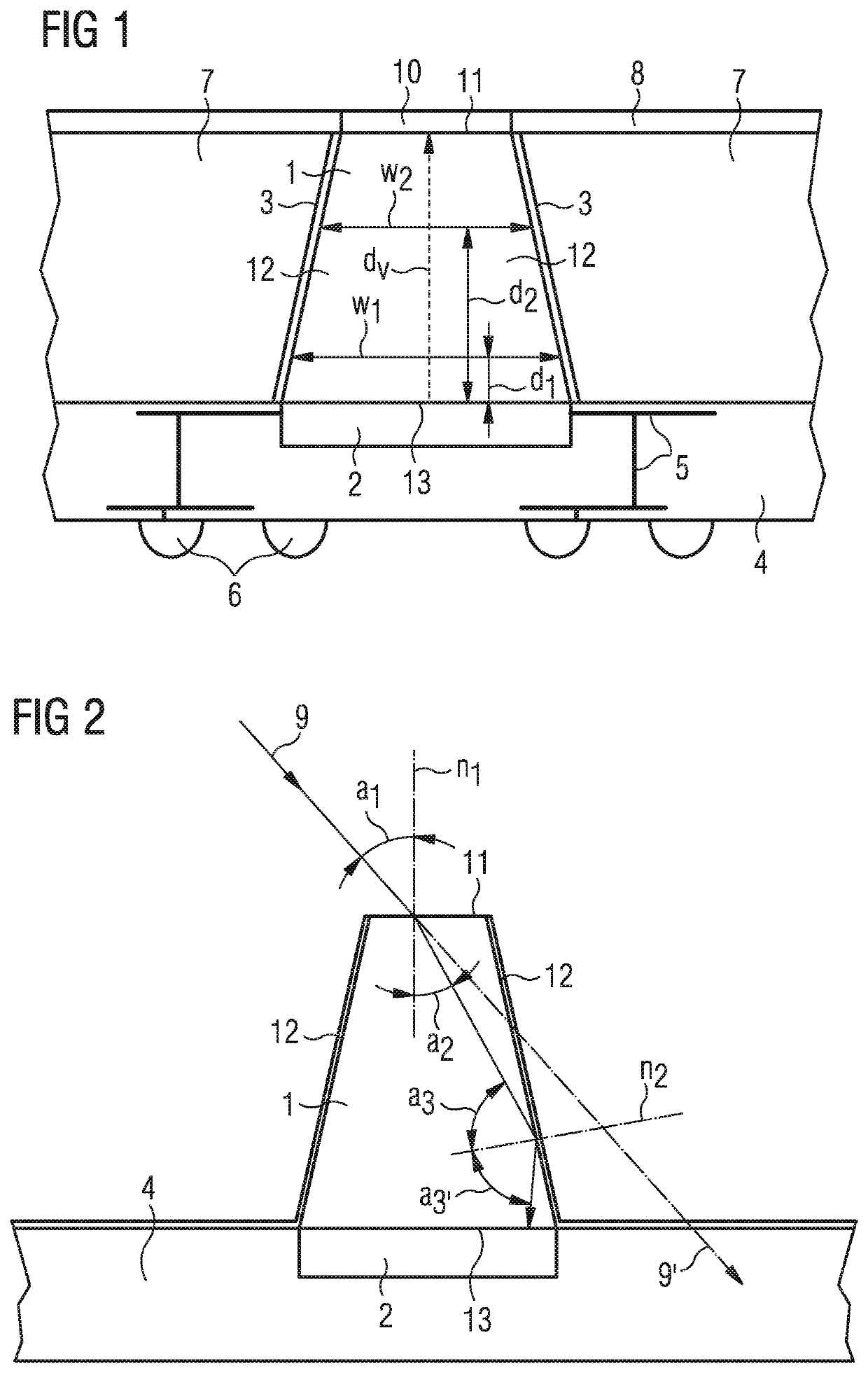
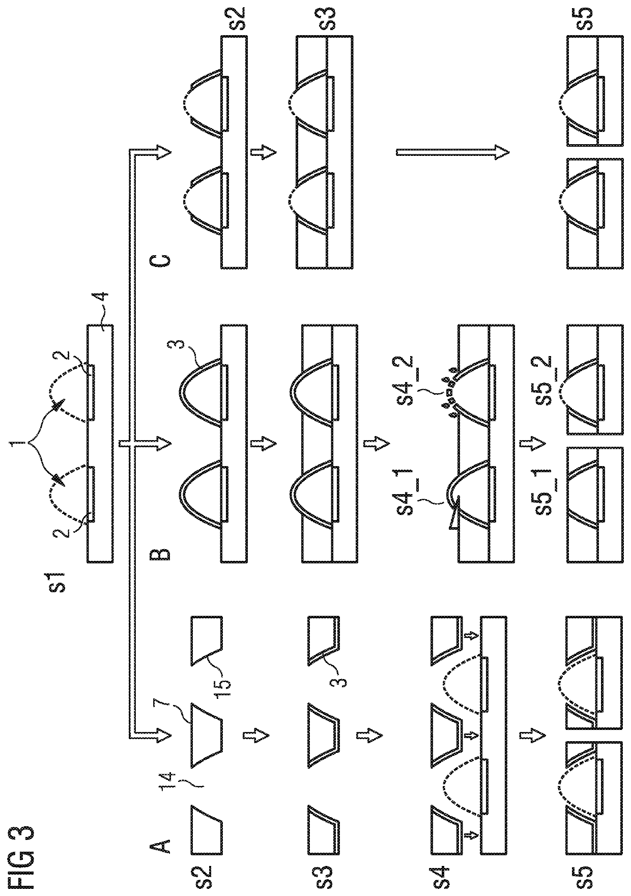
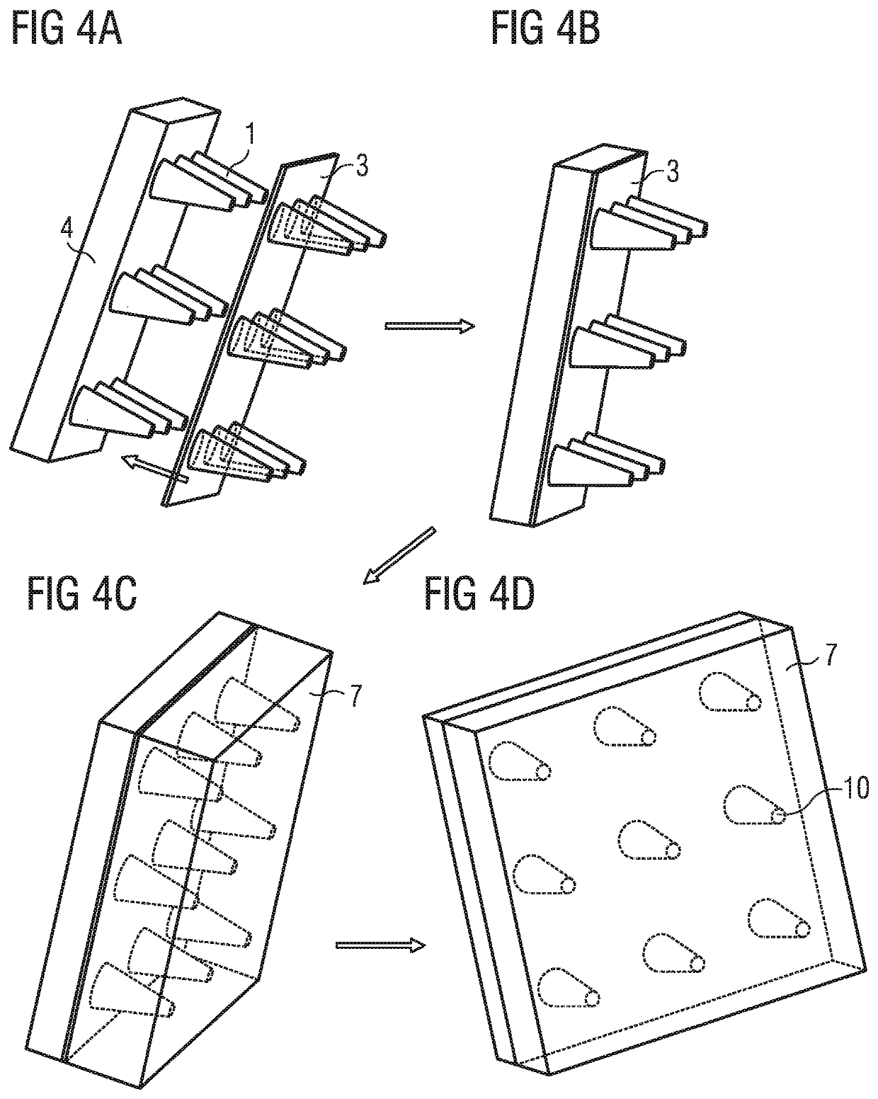
[0056]FIG. 1 shows a cross section of an example embodiment of an optical package. The optical package comprises a carrier 4, an optoelectronic component 2, an aspheric lens 1, and a reflective layer 3.

[0057]The carrier 4 comprises electrical interconnections 5. In this particular embodiment these are implemented as through substrate vias or wiring and electrically connect the optoelectric component 2 with an underside of the carrier 4. Bump contacts 6 are arranged at the underside of the carrier 4 for external electric connection of the optical package. The carrier 4 may be a semiconductor substrate, for example a wafer, so that the optical package can be produced in a CMOS process at the wafer level minimizing footprint and assembly costs. The carrier 4 may instead be any other carrier suitable for optoelectronic packages, like a printed circuit board, for instance.

[0058]The optoelectric component 2 is mounted on or into the carrier 4 using semiconductor technology, for example. G...


PUM

PropertyMeasurementUnit
taper angleaaaaaaaaaa
reflectivityaaaaaaaaaa

Abstract

An optical package is proposed comprising a carrier, an optoelectronic component, an aspheric lens, and a reflective layer. The carrier comprises electrical interconnections and the optoelectric component is arranged for emitting and / or detecting electromagnetic radiation in a specified wavelength range. Furthermore, the optoelectric component is mounted on the carrier or integrated into the carrier and electrically connected to the electric interconnections. The aspheric lens has an upper surface, a lateral surface, and a bottom surface and the bottom surface is arranged on or near the optoelectric component. The aspheric lens comprises a material which is at least transparent in the specified wavelength range. The reflective layer comprises a reflective material, wherein the reflective layer at least partly covers the lateral surface of the aspheric lens, and wherein the reflective material is at least partly reflective in the specified wavelength range.

Description

[0001]This invention relates to an optical package and to a method of producing an optical package.BACKGROUND OF THE INVENTION[0002]Existing optical sensor packages typically employ optical interference filters and often must fulfil conflicting requirements. Ambient Light Sensing (ALS) applications, for example, often seek to have a wide angular field of view, yet a small range of incident angles on filter and sensor. For example, interference filters often have issues with progressively larger wavelength shifts in their spectral response curves as the incident light impinges at increasing off-axis angles.[0003]A conventional approach to solving this problem is through the use of a small diffuser aperture placed near the outer surface of the device that the sensor is embedded in, e.g. a cell phone or tablet, while using a large air gap between sensor and aperture, such that the angle of view, from the standpoint of the interference filter covering the sensor, subtends a much smaller...

Claims


Application Information

Patent Timeline
Patent Type & Authority Patents(United States)
IPC IPC(8): H01L31/0232H01L27/146H01L33/46H01L33/62G02B19/00H01L31/02H01L31/18H01L33/00H01L33/56H01L33/60H01L33/58H01L31/0203G02B3/04
CPCH01L27/14618G02B19/0028H01L31/02005H01L31/02327G02B3/04H01L33/0095H01L27/14625G02B19/0061H01L27/14683H01L33/56G02B19/0076H01L27/14685H01L33/60H01L31/1876H01L31/0203H01L33/46H01L33/58H01L33/62H01L31/0232H01L2933/0066H01L2933/005H01L27/14623H01L2933/0058
Inventor MEHRL, DAVIDBODNER, THOMASTOSCHKOFF, GREGORETSCHMAIER, HARALDSCHRANK, FRANZ
Owner AMS AG
Features
  • R&D
  • Intellectual Property
  • Life Sciences
  • Materials
  • Tech Scout
  • Unparalleled Data Quality
  • Higher Quality Content
  • 60% Fewer Hallucinations
Learn More