[0017]According to a further embodiment, a contact metallization is applied to the bottom side of the substrate. The contact metallization can be designated and embodied, for example, for mounting and / or electrically contacting the semiconductor chip from the bottom side. The contact metallization can comprise for this purpose one or more metals selected from Al, Ag, Au, Pt, Ti, Sn, In, Ni, Cu, Rh and Ir as well as alloys and / or mixtures and / or layer combinations thereof. The contact metallization can preferably have a thickness of a few micrometers, for example, greater than or equal to 2 μm and less than or equal to 4 μm. In particular, the contact metallization can comprise in the first lateral direction, adjacent to the bottom side of the substrate, a width which is equal to width B3. This can mean, in particular, that the contact metallization, at least in the first lateral direction and preferably in all lateral directions, does not protrude beyond the bottom side area of the substrate. Compared to the width of the substrate at half height and the width at the top side of the substrate, the contact metallization can thus be retracted in the lateral direction. If a plurality of semiconductor chips, thus two or more semiconductor chips, is mounted on a carrier, wherein each of the semiconductor chips is mounted on the carrier with the carrier-facing bottom side by means of a connecting layer, directly adjacent semiconductor chips can have a minimum distance A1 to each other, respectively, while the connecting layers of directly adjacent semiconductor chips, according to the extents of the bottom sides and / or the contact metallizations of the semiconductor chips, have a minimum distance A2, wherein the following applies: A1<A2. In other words, the contact metallizations and thus also the connecting layers intended for mounting are spaced apart from each other to a greater extent than the minimum distance between the semiconductor chips, even in case of closely arranged semiconductor chips, so that unwanted electrical connections between adjacent semiconductor chips caused by too closely spaced connecting layers can be avoided. As a result, the risk of so-called electrical bridging can be avoided, even in tightly arranged multi-chip applications.
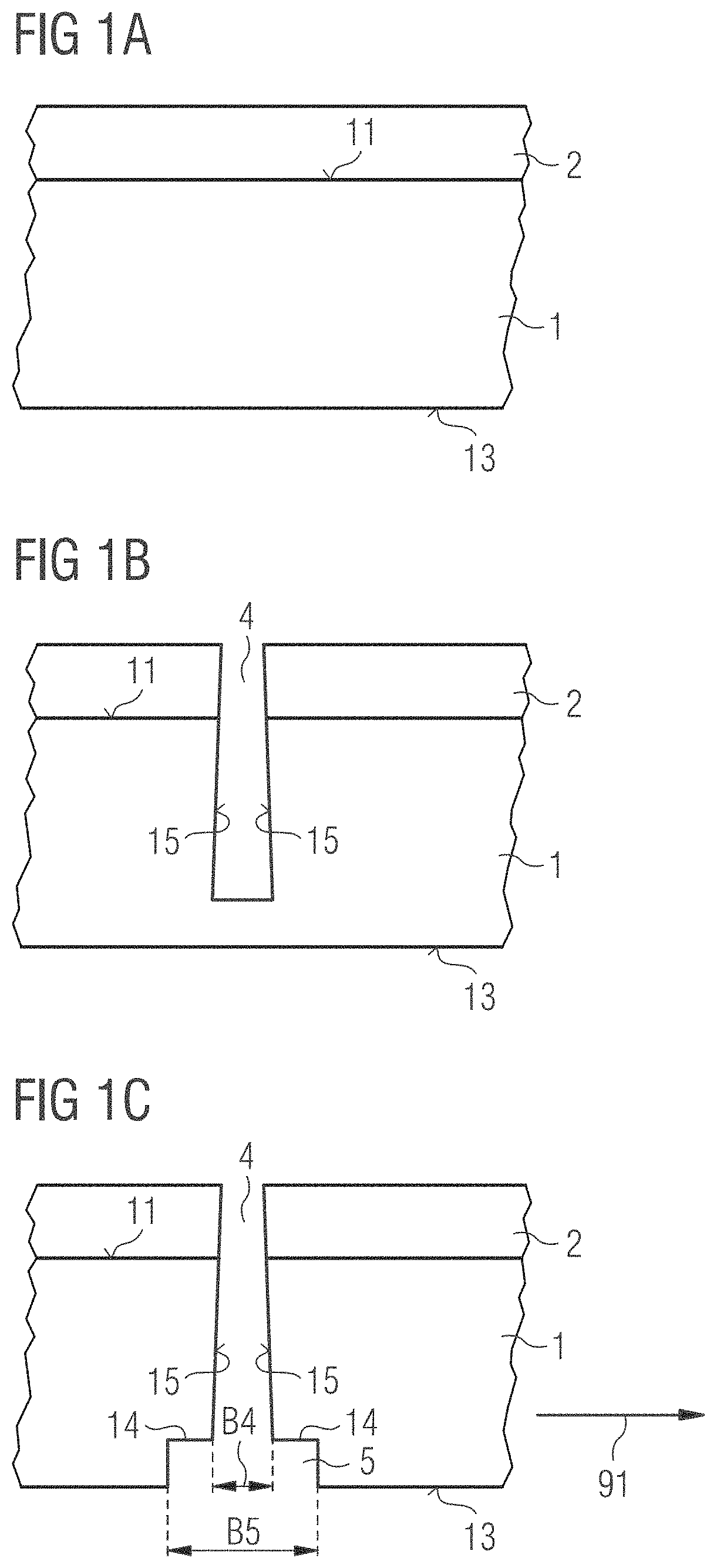
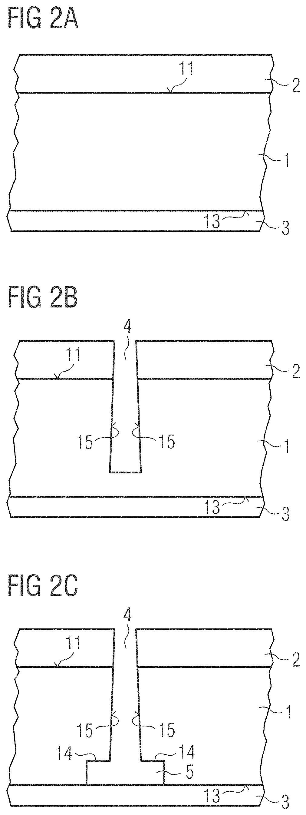
[0026]By means of the method described here, a separation of the substrate wafer and thus a chip singulation is possible by means of an etching process instead of a conventional laser separation method. By avoiding the disadvantages of laser separation methods, for example, the breaking strength of the semiconductor chips produced in this way can be significantly increased. In particular, the breaking strength of semiconductor chips can be increased with substrates whose thermal expansion coefficient is not matched to the thermal expansion coefficient of the semiconductor material of the semiconductor layer, since, compared to laser separation methods, no significant heating during singulation takes place. In addition, it may be possible to produce a very small undercut, in particular of less than or equal to 5 μm, or no undercut at all in the substrate wafer and thus the substrate on the side facing the semiconductor.
[0027]By means of the two-stage etching process a partial broadening of the separation trench, in particular in the region of the interface to the contact metallization on the bottom side of the substrate wafer, is produced, so that a semiconductor chip is produced whose substrate, in the manner described above, is wider at the side facing the semiconductor layer than at the side facing away from the semiconductor layer. In particular, the difference in the width of the substrate between the side facing the semiconductor layer and the half height is preferably significantly smaller than the difference between the width of the substrate at half height and the width of the substrate on the side facing away from the semiconductor layer. Thus, at the same time a contact metallization on the bottom side of the substrate is drawn back compared to the chip top edge. This can also generate a reservoir for excess material of a connecting layer, i.e., for example, a solder metal or an adhesive, whereby, for example, in the case of a solder metal, a reduction of the so-called “solder bulgings” can be achieved. In addition, by the described etching process, the side surface and the chip edge are free of typical damages caused by laser cutting, so that, as described, the breaking force of the semiconductor chips can be significantly increased.
[0028]Since, as a result of the process during the first etching process, a fluoropolymer is deposited as a passivation on the side surfaces of the semiconductor chip, a protection of the side surfaces of the semiconductor chip can be achieved. Furthermore, the passivation can deliberately be used and / or modified to increase the adhesion and surface wetting of, for example, adhesive, solder, potting or lens materials such as epoxy, silicone and the like. In addition, it may also be possible to remove the passivation at least in places or completely from the chip side surfaces.

