Method for driving solid-state imaging device

a solid-state imaging and driving technology, applied in the direction of radiation controlled devices, distance measurement, instruments, etc., can solve the problems of difficult to achieve downsizing, increase the range of distance measurement, and decrease the resolution of distance, so as to achieve high distance measurement accuracy

Active Publication Date: 2021-02-23
NUVOTON TECH CORP JAPAN
View PDF14 Cites 0 Cited by
  • Summary
  • Abstract
  • Description
  • Claims
  • Application Information

AI Technical Summary

Benefits of technology

[0008]In view of the abovementioned problems, the present disclosure has an object to provide a method for driving a solid-state imaging device which is small, has high distance measurement accuracy, and obtains a distance measurement signal that covers a wide distance measurement range.
[0010]With the method for driving a solid-state imaging device according to the present disclosure, a small solid-state imaging device can obtain a distance measurement signal that covers a wide distance measurement range with high distance measurement accuracy.

Problems solved by technology

Meanwhile, in PTL 1, when a pixel that obtains background light is taken into account, a distance is calculated using three pixels as one distance measurement unit, and thus one distance measurement unit for calculating a distance is large, meaning that downsizing is difficult to achieve.
Furthermore, since each pixel includes only one charge accumulator, an increase in the pulse width (To) of the light source leads to an increase in distance measurement range D, but causes a decrease in distance resolution.

Method used


Image

  • Method for driving solid-state imaging device
  • Method for driving solid-state imaging device
  • Method for driving solid-state imaging device

Examples


embodiment 1

[0074][1-1. Configuration of Solid-State Imaging Device]

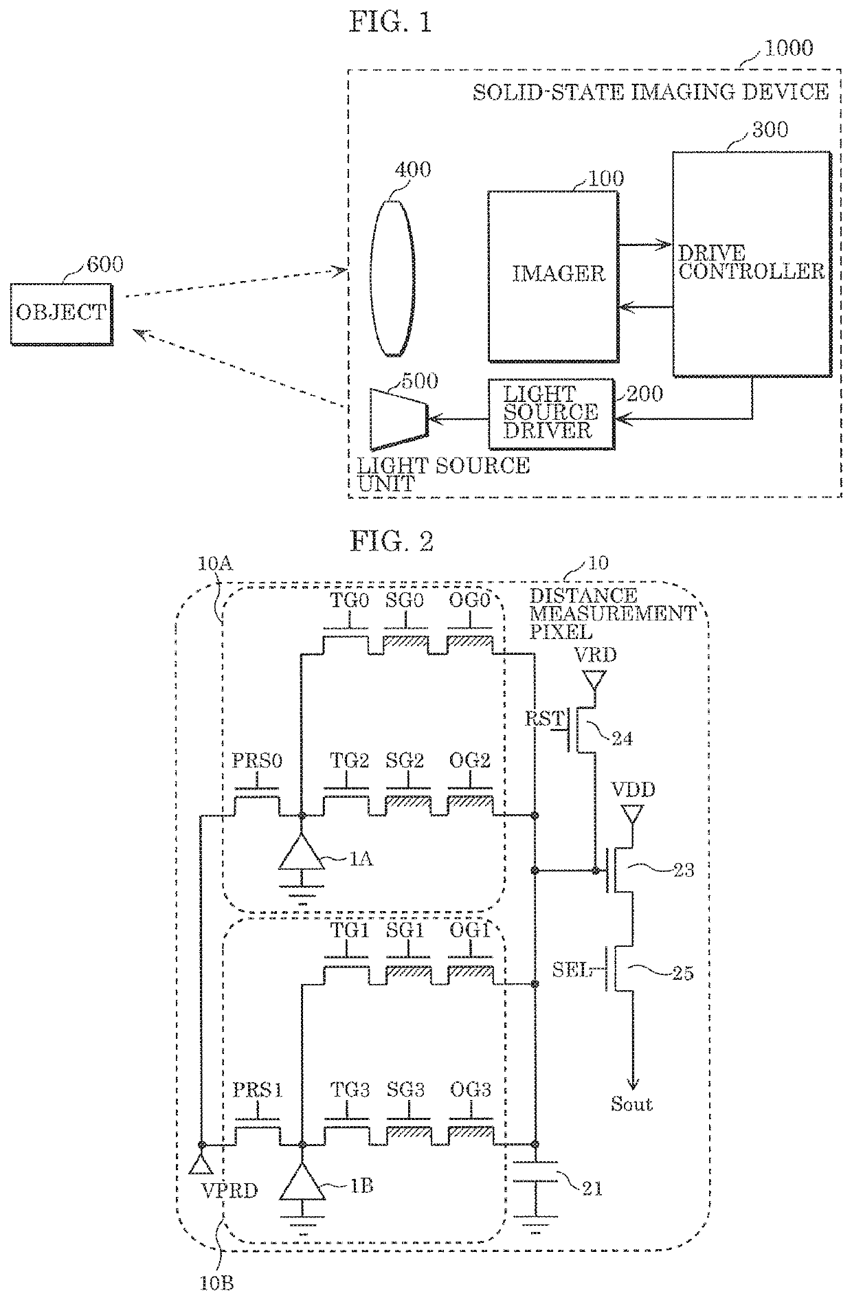
[0075]FIG. 1 is a function block diagram illustrating an example of an outline configuration of solid-state imaging device 1000 according to Embodiment 1. As illustrated in this figure, solid-state imaging device 1000 includes imager 100, light source driver 200, drive controller 300, optical lens 400, and light source unit 500.

[0076]Solid-state imaging device 1000 according to the present embodiment functions as a distance measurement imaging device which measures the distance to object 600, by emitting infrared light or the like from light source unit 500 toward object 600 and receiving, by imager 100, light reflected from object 600.

[0077]Light source driver 200 generates a light emission signal instructing light irradiation to object 600.

[0078]In accordance with the light emission signal generated by drive controller 300, light source unit 500 irradiates object 600 with light using a light emission current generated by ligh...

embodiment 2

[0145][2-1. Configuration of Distance Measurement Pixel]

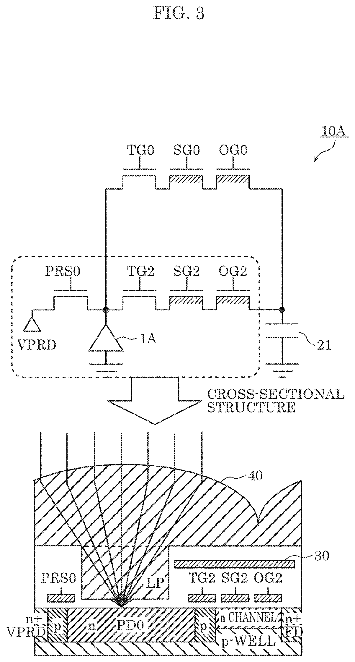
[0146]FIG. 8 illustrates a circuit configuration of a distance measurement pixel of a solid-state imaging device according to Embodiment 2. As illustrated in FIG. 8, distance measurement pixel 11 includes: one unit pixel 11A which receives reflected light, photoelectrically converts the reflected light into signal charge, and accumulates and outputs the signal charge; one FD 21 which converts the signal charge into a voltage; reset (RST) transistor 24 which discharges the signal charge of FD 21 to a reset drain (VRD); amplification transistor 23 which is connected to a VDD power supply and amplifies a signal from FD 21; and selection (SEL) transistor 25 which outputs and controls a signal from amplification transistor 23 in accordance with an exteriorly obtained selection signal.

[0147]One unit pixel 11A includes: one light receiver which receives the reflected light and photoelectrically converts the received light; one charge ...


PUM

PropertyMeasurementUnit
speedaaaaaaaaaa
chargeaaaaaaaaaa
distanceaaaaaaaaaa

Abstract

Provided is a method for driving a solid-state imaging device including a unit pixel which includes at least a first pixel including: a photoelectric converter which receives reflected light from an object and converts the reflected light into charge; an exposure resetter which switches between exposure and discharge of the charge in the photoelectric converter; and a plurality of readers which read the charge from the photoelectric converter and include at least a first reader and a second reader. The method includes: performing a first exposure as the exposure that is performed in a first period in which a gate of the first reader is ON; and performing a second exposure as the exposure that is performed in a second period which is started in conjunction with the end of the first period and in which a gate of the second reader is ON.

Description

CROSS REFERENCE TO RELATED APPLICATIONS[0001]This application is a U.S. continuation application of PCT International Patent Application Number PCT / JP2016 / 003494 filed on Jul. 28, 2016, claiming the benefit of priority of Japanese Patent Application Number 2015-154512 filed on Aug. 4, 2015, the entire contents of which are hereby incorporated by reference.BACKGROUND1. Technical Field[0002]The present disclosure relates to methods for driving solid-state imaging devices to be used in imaging for distance measurement.2. Description of the Related Art[0003]Among methods for sensing an object, the time of flight (TOF) method is known in which a distance is measured using flight time that light takes to travel to and return from a measurement object.[0004]Japanese Unexamined Patent Application Publication No. 2004-294420 (Patent Literature 1) discloses a distance image sensor in which two different signal storage units store signals obtained by transfer of charge with different phases in...

Claims


Application Information

Patent Timeline
Patent Type & Authority Patents(United States)
IPC IPC(8): G01C3/08G01S7/486G01S17/89H04N5/374H04N5/353H01L27/146G01S7/4863G01S7/4865G01S17/10G01S7/4861H01L27/148H04N5/235G01S17/894
CPCG01S7/4868G01S7/4861G01S7/4863G01S7/4865G01S17/10G01S17/89H01L27/146H01L27/14818H01L27/14856H04N5/2351H04N5/353H04N5/374G01S17/894H04N25/53H04N25/76H04N23/71
Inventor YAMADA, TOHRUSUZUKI, SEISHIMIZU, YASUYUKI
Owner NUVOTON TECH CORP JAPAN
Why Eureka
Try Eureka