Solid-state imaging device

a solid-state imaging and imaging device technology, applied in the direction of radiological control devices, instruments, television systems, etc., can solve the problems of reduced sensitivity, reduced distance measurement accuracy, and complex circuitry, and achieve high distance measurement accuracy

Active Publication Date: 2020-05-26
PANASONIC SEMICON SOLUTIONS CO LTD
View PDF14 Cites 0 Cited by
  • Summary
  • Abstract
  • Description
  • Claims
  • Application Information

AI Technical Summary

Benefits of technology

[0009]In view of the abovementioned problems, the present disclosure has an object to provide a solid-state imaging device which is small, has high distance measurement accuracy, and obtains a distance measurement signal that covers a wide distance measurement range.
[0011]According to the present disclosure, a small solid-state imaging device can obtain a distance measurement signal that covers a wide distance measurement range with high distance measurement accuracy.

Problems solved by technology

In other words, the distance measurement accuracy is inversely proportional to the pulse width (Tp) of the light source; there is the problem that when the pulse width of the light source is increased in order to widen the distance measurement range (limit) D, conversely, the distance measurement accuracy is decreased.
Furthermore, the exposure period is determined according to the TX width, and therefore, in the case where the pulse width of the light source is reduced, the TX width is reduced, and there is a need to increase three TX wiring widths for suppressing a pulse wiring delay; thus, there is the problem that sensitivity is reduced, for example, because mechanical vignetting of incident light due to wiring occurs.
In (c), the circuitry is complex, and it is not possible to obtain a sufficient aperture ratio in this case either.
Thus, there is the problem that miniaturization of pixels, that is, if the number of pixels is the same, downsizing, and if the optical size is the same, an increase in resolution, is difficult.
Furthermore, (b) has the problem that the distance measurement accuracy is decreased because the background light is different between two images.

Method used


Image

  • Solid-state imaging device
  • Solid-state imaging device
  • Solid-state imaging device

Examples


embodiment 1

[0043][1-1. Configuration of Distance Measurement Imaging Device]

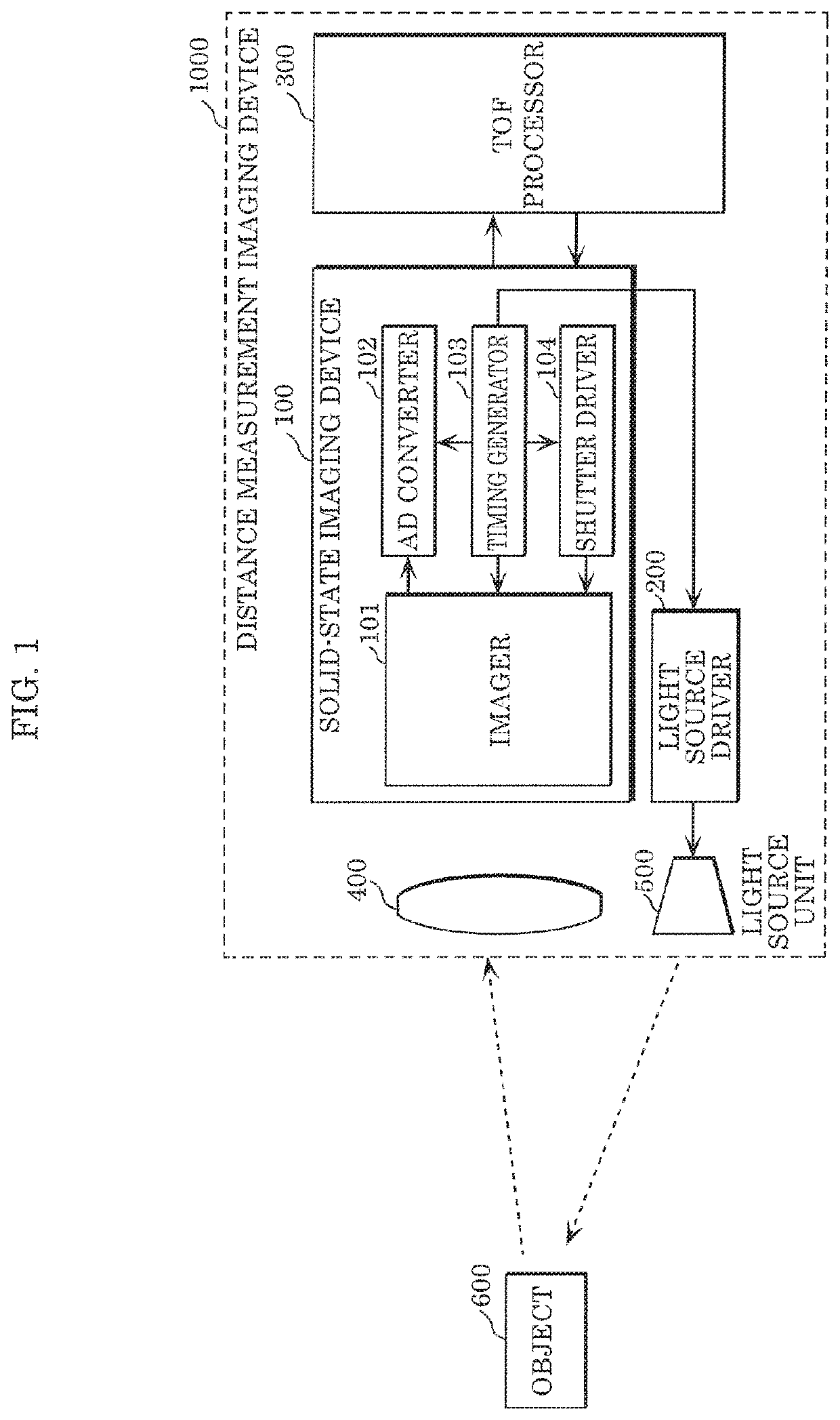
[0044]FIG. 1 is a function block diagram illustrating an example of an outline configuration of distance measurement imaging device 1000 according to Embodiment 1. As illustrated in this figure, distance measurement imaging device 1000 includes solid-state imaging device 100, light source driver 200, TOF processor 300, optical lens 400, and light source unit 500. Solid-state imaging device 100 includes imager 101, AD converter 102, timing generator 103, and shutter driver 104.

[0045]Timing generator 103 generates a light emission signal instructing light irradiation to object 600 to drive light source unit 500 via light source driver 200, and generates an exposure signal instructing exposure to light reflected from object 600.

[0046]Imager 101 performs exposure on a region including object 600 plural times according to timing indicated by the exposure signal generated by timing generator 103, and obtains a signal corresp...

embodiment 2

[0133]A solid-state imaging device and a method for driving the same according to Embodiment 2 will be described, focusing on differences from Embodiment 1.

[0134]FIG. 15 is a timing chart illustrating a method for driving a solid-state imaging device according to Embodiment 2. FIG. 16 is a schematic plan view of the imaging region for explaining that a different exposure control is performed for each pixel row in the solid-state imaging device according to Embodiment 2.

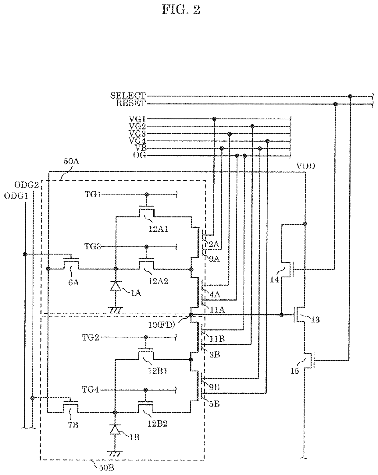
[0135]In solid-state imaging device 100 according to Embodiment 1, only drive pulse signal ODG in the exposure controller is different between pixel 50A (the first pixel group) and pixel 50B (the second pixel group). The reflectance of object 600 has a large impact on a TOF distance measurement imaging device using near infrared light. When object 600 has low reflectance, the reflected light is weak, and therefore it is necessary to increase light source power or increase the length of the exposure period, but in the ...

embodiment 3

[0140]A solid-state imaging device and a method for driving the same according to Embodiment 3 will be described, focusing on differences from Embodiments 1 and 2.

[0141]FIG. 18 is a schematic plan view illustrating a layout configuration of pixels of the solid-state imaging device according to Embodiment 3. The solid-state imaging device according to the present embodiment is different from solid-state imaging device 100 according to Embodiment 1 only in that light-shielding films 20A and 20B are formed in the imaging region. In the solid-state imaging device according to the present embodiment, light-shielding film 20A is provided so as to cover charge accumulators 2A and 4A and transfer controller 9A, and light-shielding film 20B is provided so as to cover charge accumulators 3B and 5B and transfer controller 9B.

[0142]With only a metal wiring layer as in a normal CMOS process, even when upper wiring shields light, oblique incident light enters the charge accumulator and is photoel...


PUM

PropertyMeasurementUnit
speedaaaaaaaaaa
direct-current potentialaaaaaaaaaa

Abstract

A plurality of pixels of a solid-state imaging device include: a photoelectric converter which receives light from an object and converts the light into charge; a plurality of readers which read the charge from the photoelectric converter; a plurality of charge accumulators each of which accumulates the charge of the photoelectric converter read from the plurality of readers; and a transfer controller which performs a transfer control including controlling whether the charge accumulated in one of the plurality of charge accumulators is transferred or blocked from being transferred to another one of the plurality of charge accumulators. The transfer controller is disposed between the plurality of charge accumulators.

Description

CROSS REFERENCE TO RELATED APPLICATIONS[0001]This application is a U.S. continuation application of PCT International Patent Application Number PCT / JP2016 / 003493 filed on Jul. 28, 2016, claiming the benefit of priority of Japanese Patent Application Number 2015-154552 filed on Aug. 4, 2015, the entire contents of which are hereby incorporated by reference.BACKGROUND1. Technical Field[0002]The present disclosure relates to solid-state imaging devices to be used in imaging for distance measurement.2. Description of the Related Art[0003]Among methods for sensing an object, the time of flight (TOF) method is known in which a distance is measured using flight time that light takes to travel to and return from a measurement object.[0004]Japanese Unexamined Patent Application Publication No. 2004-294420 (Patent Literature 1) discloses the related art in which two different signal storage units store signals obtained by transfer of charge with different phases in synchronization with interm...

Claims


Application Information

Patent Timeline
Patent Type & Authority Patents(United States)
IPC IPC(8): H04N5/243H01L27/146G01S17/89H04N5/33G01S7/481H04N5/378G01S7/4863G01S17/894
CPCH01L27/14645H01L27/14623H01L27/146H04N5/243H01L27/14636H01L27/14649H04N5/378H01L27/14607G01S17/89G01S7/4863G01S7/4816H04N5/332G01S17/894H04N23/11H04N23/76H04N25/75
Inventor SUZUKI, SEIYAMADA, TOHRUSHIMIZU, YASUYUKI
Owner PANASONIC SEMICON SOLUTIONS CO LTD
Why Eureka
Try Eureka