Multi-beam electron microscope

a multi-beam, electron microscope technology, applied in the field of electron microscopes, can solve problems such as problems and challenges

Active Publication Date: 2021-03-02
FEI CO
View PDF3 Cites 2 Cited by
  • Summary
  • Abstract
  • Description
  • Claims
  • Application Information

AI Technical Summary

Benefits of technology

[0014]In one embodiment, an electron microscope comprises specimen holder, for holding a specimen; an electron beam column, for producing an array of electron beams and concurrently irradiating an array of target areas of said specimen therewith; a scanning assembly, for producing relative scanning motion of said beam array with respect to the specimen; and a detector, for detecting radiation emanating from the specimen in response to said irradiation, characterized in that said detector is a backscattered electron detector that can be disposed proximal to the specimen at a side thereof facing said electron beam column; provided with an array of apertures that allow passage of said electron beams from said column to the specimen; and provided with a functionally sub-divided detection surface that enables segregated detection of a backscattered electron flux produced by each individual beam. In this way, the backscattered electrons from each electron beam may be detected.

Problems solved by technology

However, the concurrent use of multiple imaging beams (beamlets; sub-beams; component beams) also presents various technical problems and challenges, which need to be addressed satisfactorily.

Method used


Image

  • Multi-beam electron microscope
  • Multi-beam electron microscope
  • Multi-beam electron microscope

Examples


embodiment 1

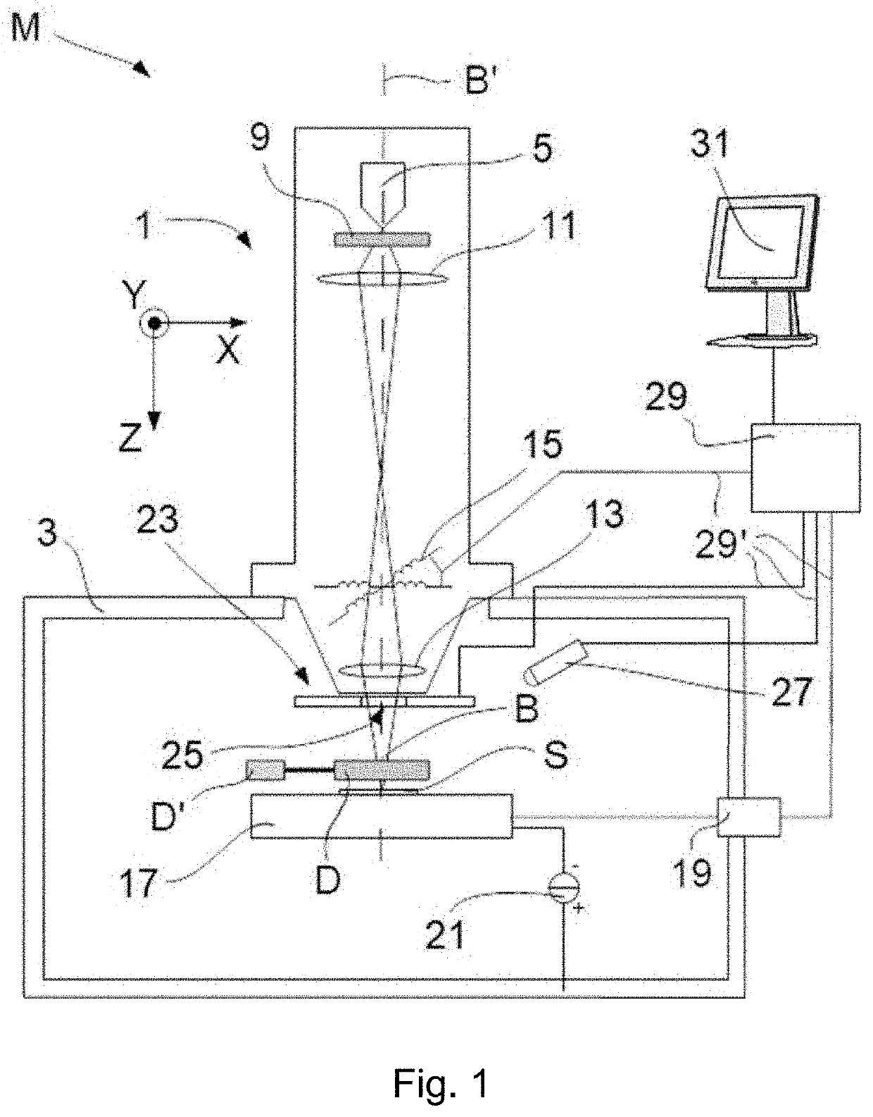
[0055]FIG. 1 (not to scale) is a highly schematic depiction of an embodiment of an electron microscope M in which the present invention can be exploited; more specifically, it shows an embodiment of a SEM (though, in the context of the current invention, it could also be a STEM, for example). The microscope M comprises an electron beam column / illuminator 1, which produces an electron beam that propagates along a particle-optical axis B′. The electron beam column 1 is mounted on a vacuum chamber 3, which comprises a specimen holder 17 and associated stage / actuator 19 for holding / positioning a specimen S. The vacuum chamber 3 is evacuated using vacuum pumps (not depicted). With the aid of voltage source 21, the specimen holder 17, or at least the specimen S, may, if desired, be biased (floated) to an electrical potential with respect to ground.

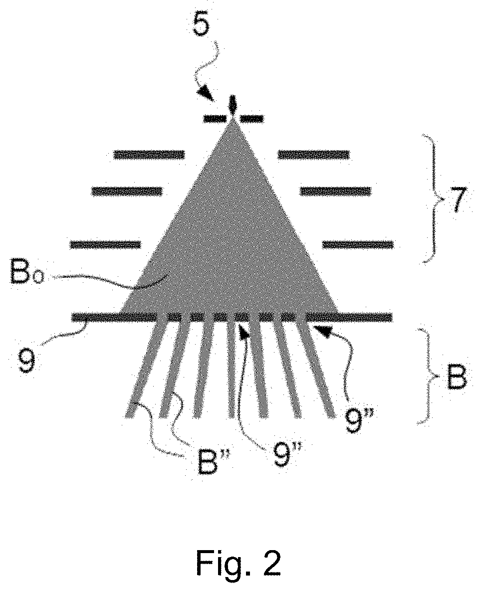
[0056]The electron beam column 1 comprises an electron source 5 (such as a Schottky emitter, cold FEG or LaB6 filament, for example), lenses 11...

embodiment 2

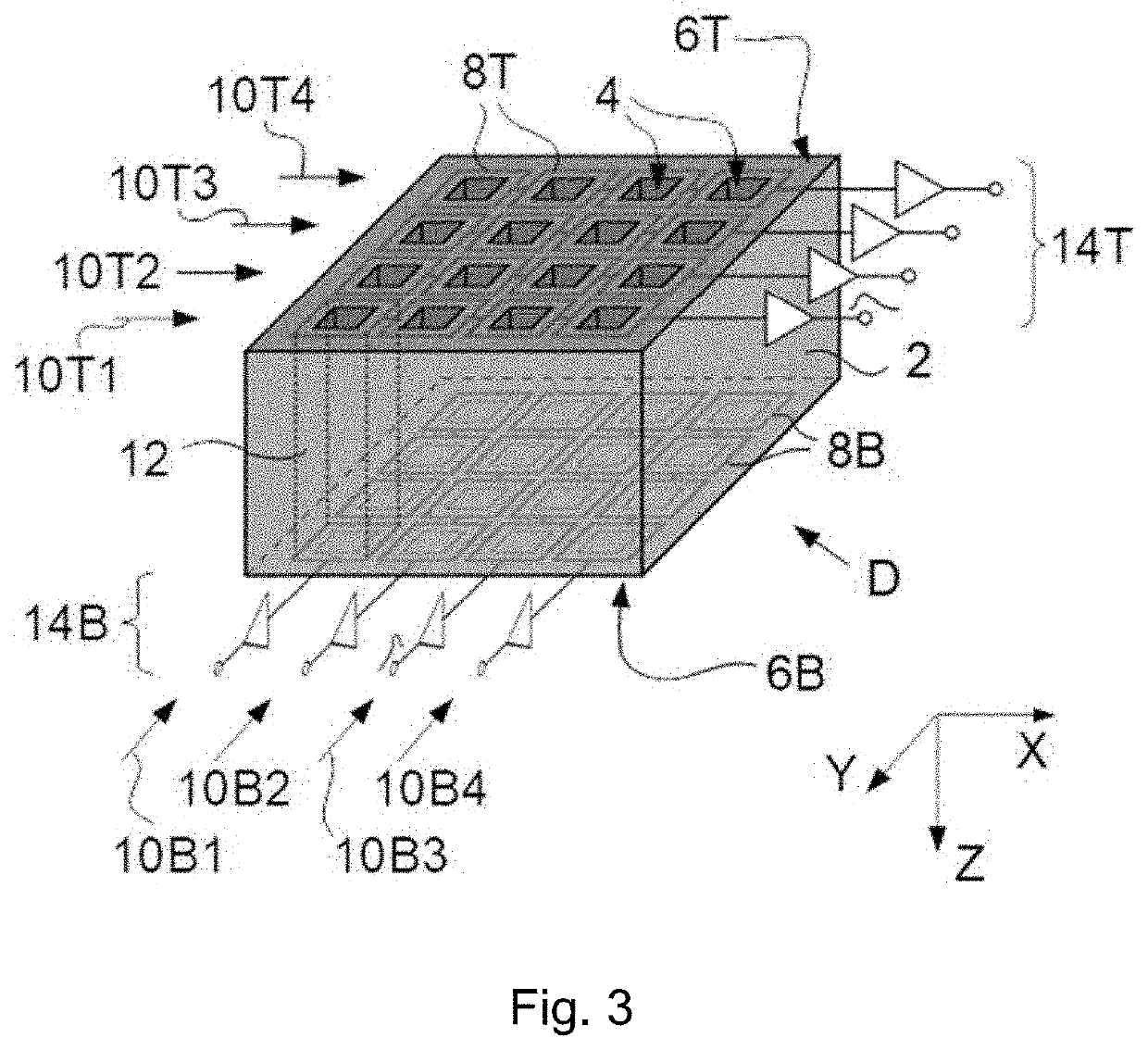
[0074]FIG. 4 shows an alternative embodiment of the present invention, in which the employed detector (D1, D2, D3, D4) has a different architecture and operating mechanism. Similar to the situation illustrated in FIG. 3, the detector in the present embodiment comprises a sheet 2 (D1) in which an array of apertures 4 are present; however, in the present situation, this sheet 2 comprises scintillator material, such as a YAG (Yttrium Aluminium Garnet) scintillator, for example. As in FIG. 3, this sheet 2 is disposed proximal to the specimen S, e.g. within about five microns thereof. Explicitly shown in FIG. 4 are two primary electron beams B″1, B″2 in the array B, which respectively pass through two different apertures 41, 42 in the sheet 2 and impinge upon two different localities of the specimen S, respectively producing BSE fluxes F1, F2. These fluxes F1, F2 enter the scintillator sheet 2, where they precipitate localized photon emissions in the scintillator material in the vicinity...

embodiment 3

[0077]FIG. 5 renders a plan view of the beam array B in an embodiment of the present invention. In this particular case, the array B has an orthogonal geometry, though this does not necessarily have to be so chosen. As here depicted, a net / resultant scan direction at diagonal angle α has been selected, which gives a good packing density of the scan lines / tracts 18 traced out by the individual beams B″. Assuming the array B to comprise N×N beams B″ (N=4 in the current illustration), then one can, for example, choose:

Tan α=1 / N

One can, for example, effect the scanning motion at angle α using pure specimen motion, with beam deflection producing only a very small-amplitude deflection in a direction perpendicular hereto.


PUM

PropertyMeasurementUnit
electron microscopeaaaaaaaaaa
distanceaaaaaaaaaa
areasaaaaaaaaaa

Abstract

An electron microscope comprising:A specimen holder, for holding a specimen;An electron beam column, for producing an array of electron beams and concurrently irradiating an array of target areas of said specimen therewith;A scanning assembly, for producing relative scanning motion of said beam array with respect to the specimen;A detector, for detecting radiation emanating from the specimen in response to said irradiation,wherein said detector is:A backscattered electron detector that can be disposed proximal to the specimen at a side thereof facing said electron beam column;Provided with an array of apertures that allow passage of said electron beams from said column to the specimen;Provided with a functionally sub-divided detection surface that enables segregated detection of a backscattered electron flux produced by each individual beam.

Description

FIELD OF THE INVENTION[0001]The present invention relates to an electron microscope, and more particularly, to an electron microscope with a detector for detecting backscattered electrons from an array of electron beams.BACKGROUND OF THE INVENTION[0002]Electron microscopy is a well-known and increasingly important technique for imaging microscopic objects. Historically, the basic genus of electron microscope has undergone evolution into a number of well-known apparatus species, such as the Transmission Electron Microscope (TEM), Scanning Electron Microscope (SEM), and Scanning Transmission Electron Microscope (STEM), and also into various sub-species, such as so-called “dual-beam” apparatus (e.g. a FIB-SEM), which additionally employ a “machining” Focused Ion Beam (FIB), allowing supportive activities such as ion-beam milling or Ion-Beam-Induced Deposition (IBID), for example. More specifically:[0003]In a SEM, irradiation of a specimen by a scanning electron beam precipitates emanat...

Claims


Application Information

Patent Timeline
Patent Type & Authority Patents(United States)
IPC IPC(8): H01J37/244H01J37/20H01J37/28
CPCH01J37/244H01J37/20H01J37/28H01J2237/202H01J2237/2441H01J2237/2443H01J2237/24475H01J2237/24465
Inventor STEJSKAL, PAVELHLAVENKA, PETRSED'A, BOHUSLAV
Owner FEI CO
Why Eureka
Try Eureka