Transmission electron microscope sample preparation

a technology of electron microscope and electron microscope, which is applied in the field of electron microscope sample preparation, can solve the problems of inability to femto-laser machining, inconvenient use, and inability to achieve the effect of reducing the cost per sample, convenient use, and convenient us

Inactive Publication Date: 2005-01-11
OXFORD INSTR AMERICA
View PDF12 Cites 69 Cited by
  • Summary
  • Abstract
  • Description
  • Claims
  • Application Information

AI Technical Summary

Benefits of technology

[0030]The process of the present invention provides a safe, easy to use, semi-automated, and efficient method for cutting and extracting a specific nano-level feature from a wafer. The method allows a user to remove most of the material in situ, while also providing protection for subsequent steps. The holder or holder tip can then be placed inside a FIB for final thinning, followed by direct transfer into the TEM.
[0031]The TEM sample preparation of the present invention results in lower costs per sample. A comparison of the costs involved with TEM sample preparation using the present invention versus using other currently available methods is summarized in Table 1.

Problems solved by technology

Typical laser machining leaves thermal damage on the micrometer scale.
Since the device size scale is micrometers and less, thermal damage is unacceptable.
Femto-laser machining is not well known; however, it has been done on various materials for a couple of years.

Method used


Image

  • Transmission electron microscope sample preparation
  • Transmission electron microscope sample preparation
  • Transmission electron microscope sample preparation

Examples


Embodiment Construction

comparison of the costs involved with TEM sample preparation using the present invention versus using other currently available methods is summarized in Table 1.

[0032]These and further and other objects and features of the invention are apparent in the disclosure, which includes the above and ongoing written specification, with the claims and the drawings.

BRIEF DESCRIPTION OF THE DRAWINGS

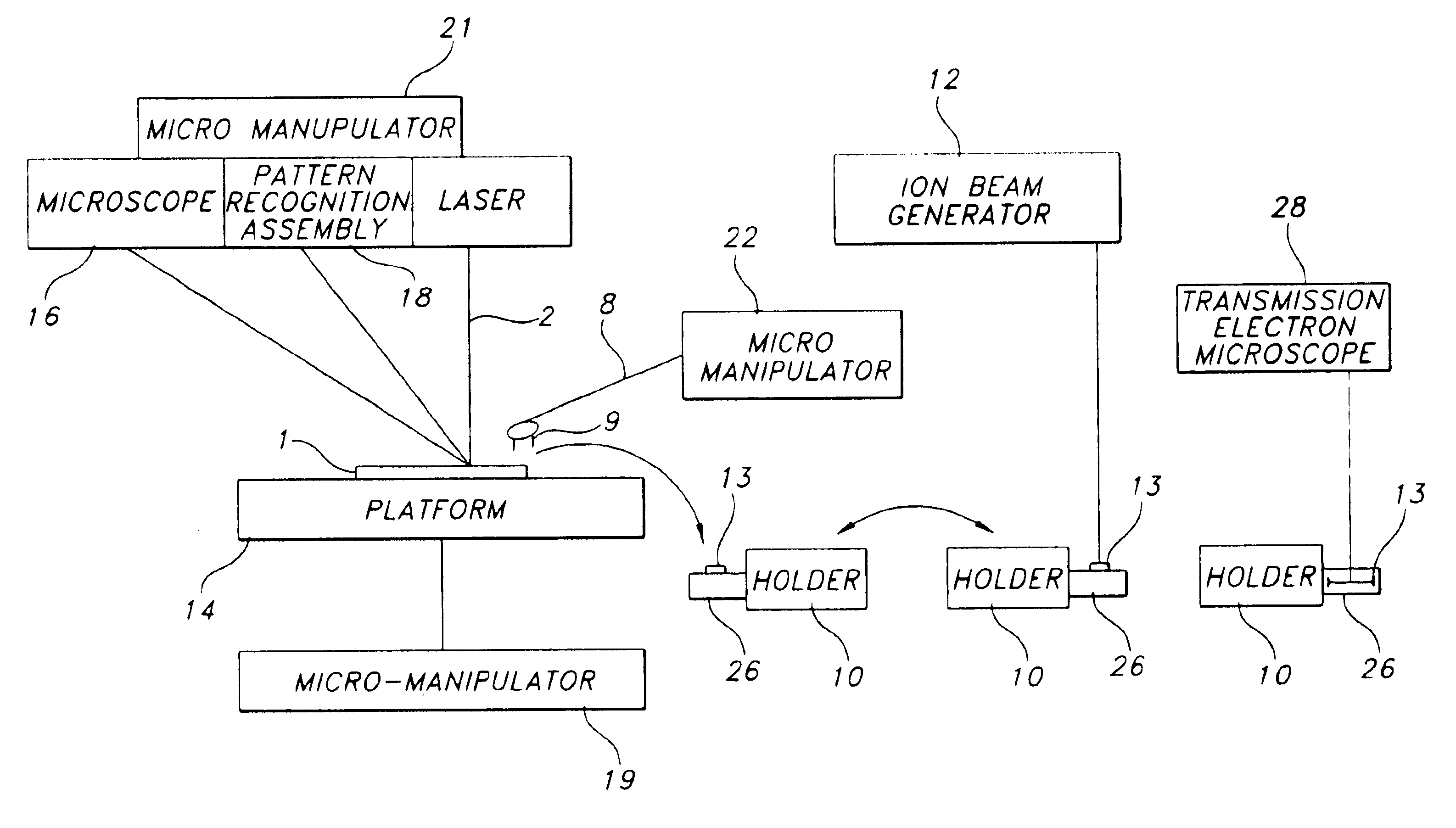
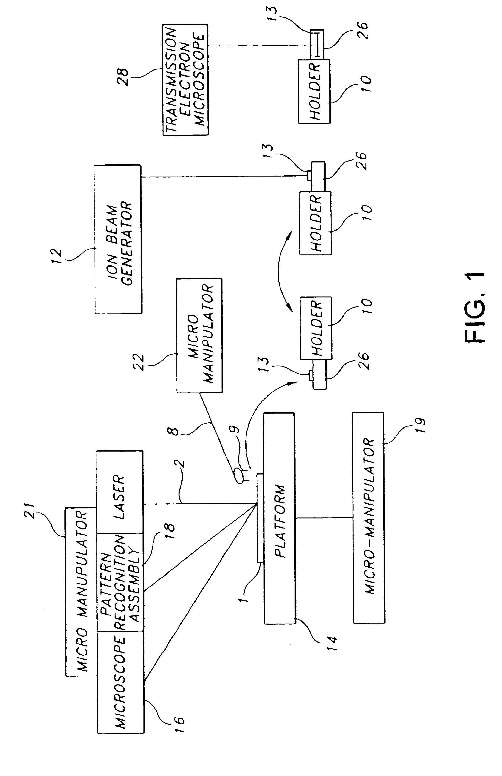
[0033]FIG. 1 is a block diagram of a preferred embodiment of the TEM sample preparation apparatus of the present invention.

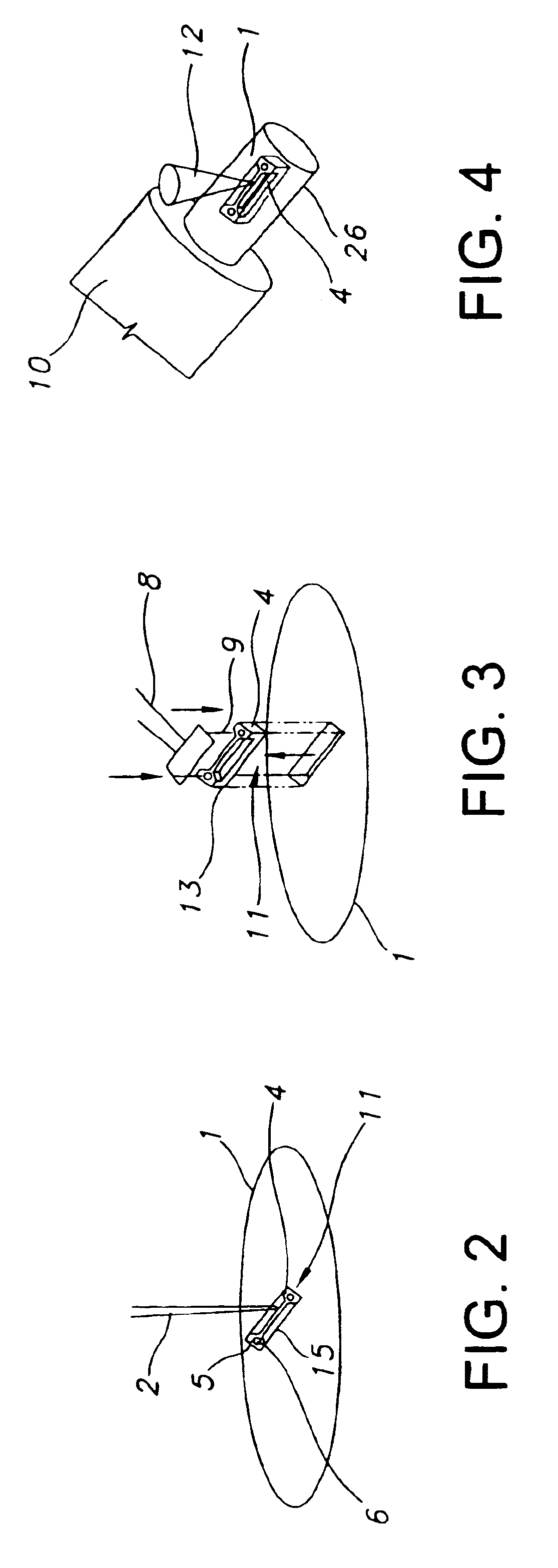
[0034]FIG. 2 is a perspective view of a laser beam cutting and drilling an area of interest from a wafer.

[0035]FIG. 3 is a perspective view of a bracket with dual stylus lifting a carrier block from a wafer.

[0036]FIG. 4 is a perspective view of a cut wafer on a TEM Holder for manipulation by an FIB.

DETAILED DESCRIPTION OF THE PREFERRED EMBODIMENTS

[0037]The process of the present invention provides a safe, easy to use, semi-automated, and efficient method for cutting and extracti...


PUM

PropertyMeasurementUnit
atomic sizeaaaaaaaaaa

Abstract

Sample preparation apparatus and method includes a wafer stage platform with an optical microscope and integrated pattern recognition to automatically address specific locations on the wafer sample of interest. A laser attaches to the optical microscope to mill a set pattern around the area of interest. A precision micro-manipulator engages the sample support structure, extracts the structure, and places the structure in a TEM holder or holder tip. The holder or holder tip can then be placed inside a FIB for final thinning, followed by direct transfer into the TEM.

Description

[0002]This application claims the benefit of U.S. Provisional Application No. 60 / 222,728 filed Aug. 3, 2000.BACKGROUND OF THE INVENTION[0003]Transmission electron microscopes (TEMs) have been used in a variety of scientific disciplines for 50 years. A TEM works in a way fundamentally similar to a light microscope except for the use of an electron beam instead of light. Electrons have a much shorter wavelength and consequently allow viewers to see features approaching atomic size (<1 nanometer) in comparison to a limit of 100 nm (0.1 μm for light).[0004]Over the last 50 years, transmission electron microscopy (TEM) technology and its applications have undergone tremendous advances. TEM has become an important analytical tool in many disciplines that require visualization and / or imaging of features less than one nanometer in size, a resolution at least two orders of magnitude greater than that available to optical microscopy.[0005]Unfortunately, the preparation of samples for TEM a...

Claims


Application Information

Patent Timeline
Patent Type & Authority Patents(United States)
IPC IPC(8): G01N1/32G01N23/225G01N23/22G21K7/00
CPCG01N1/32G01N23/225H01J2237/3174H01J2237/2817G01N2001/2886
Inventor ROBINSON, JOSEPHCHURCH, KENNETH H.
Owner OXFORD INSTR AMERICA
Why Eureka
Try Eureka