Display panel and manufacturing method thereof

a technology of display panel and manufacturing method, applied in the field of display panel, can solve the problems of low transfer efficiency, short service life of oled, low brightness, and low light utilization rate, and achieve the effects of enhancing the purity of target light emitted, reducing defects, and reducing color saturation

Active Publication Date: 2021-04-13
WUHAN CHINA STAR OPTOELECTRONICS TECH CO LTD
View PDF14 Cites 0 Cited by
  • Summary
  • Abstract
  • Description
  • Claims
  • Application Information

AI Technical Summary

Benefits of technology

[0027]The beneficial effects of the application are as follows: the present invention provides a display panel and a method of manufacturing the same. The display panel includes a plurality of sub-pixel units, at least a portion of the sub-pixel units including an excitation light source for generating an excitation light; a target light conversion layer disposed in a light exiting direction of the excitation light source for converting the excitation light into a target light; and a target light transmission layer disposed in a light exiting direction of the target light conversion layer for transmitting the target light generated by the target light conversion layer and reflecting the excitation light passing through the target light conversion layer. By disposing the target light transmission layer on the target light conversion layer, only the target light of the target light conversion layer is transmitted, and the excitation light is reflected, thus enhancing the purity of the target light emitted by the sub-pixel units, thereby alleviating the defects such as low color saturation in the existing micro-display technology to a certain extent.

Problems solved by technology

Liquid crystal displays (LCDs) and organic light-emitting diode (OLED) displays, as mainstream display devices, each have their own advantages and disadvantages that an LCD has a low light utilization rate and relatively low resolution, while an OLED has a short service life and low brightness.
However, when it is transferred to a drive substrate, transfer efficiency is low.
This method is easier to implement, but will cause mix of red, green, and blue light with near-ultraviolet light, resulting in low color saturation, and color crosstalk is likely to occur between sub-pixel units due to their large light exiting angles.
Therefore, the existing micro display technology has defects and needs to be improved.

Method used


Image

  • Display panel and manufacturing method thereof
  • Display panel and manufacturing method thereof
  • Display panel and manufacturing method thereof

Examples


Embodiment Construction

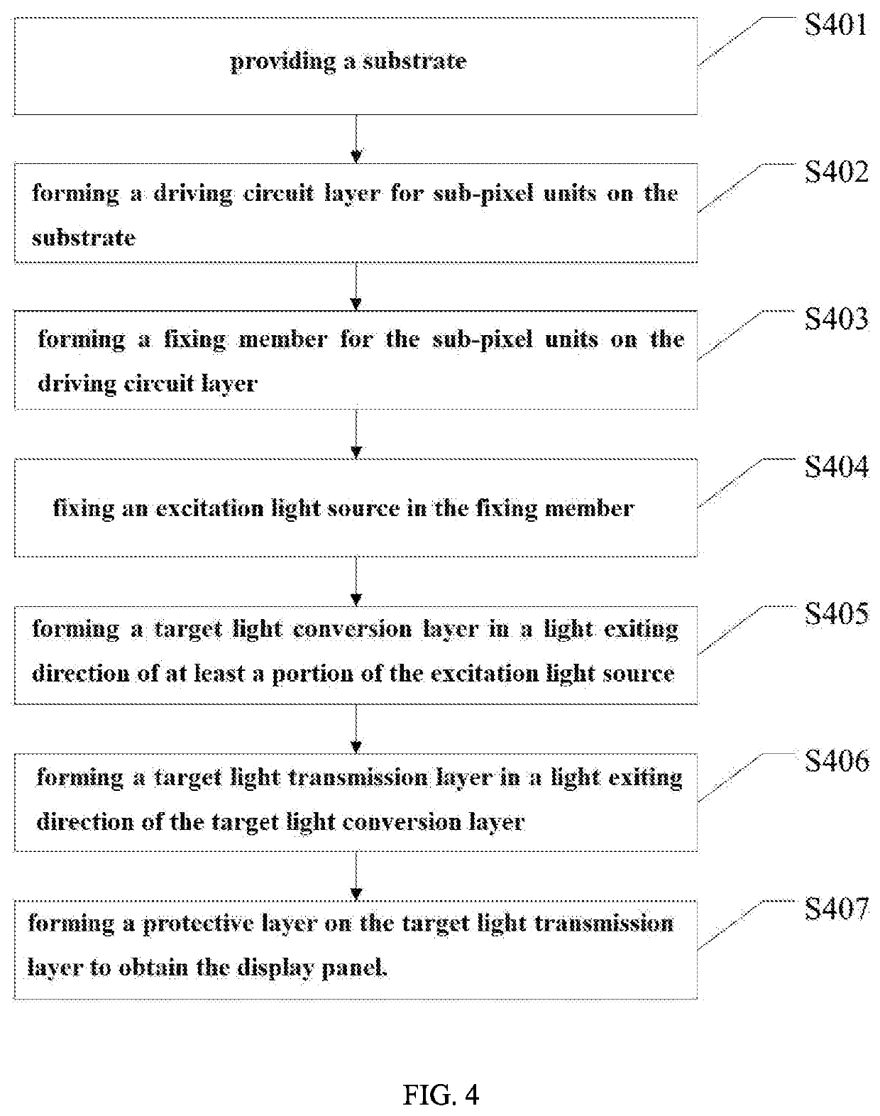
[0035]The following description of the various embodiments is provided to illustrate the specific embodiments of the invention. The spatially relative directional terms mentioned in the present invention, such as “upper”, “lower”, “before”, “after”, “left”, “right”, “inside”, “outside”, “side”, etc. and the like, may be used herein for ease of description to describe one element or feature's relationship to another element(s) or feature(s) as illustrated in the figures which are merely references. The spatially relative terms are intended to encompass different orientations in addition to the orientation as depicted in the figures.

[0036]The present invention is directed to the technical problems of the defects of the existing micro-display technology, and the embodiment of the present invention aims to solve the problems.

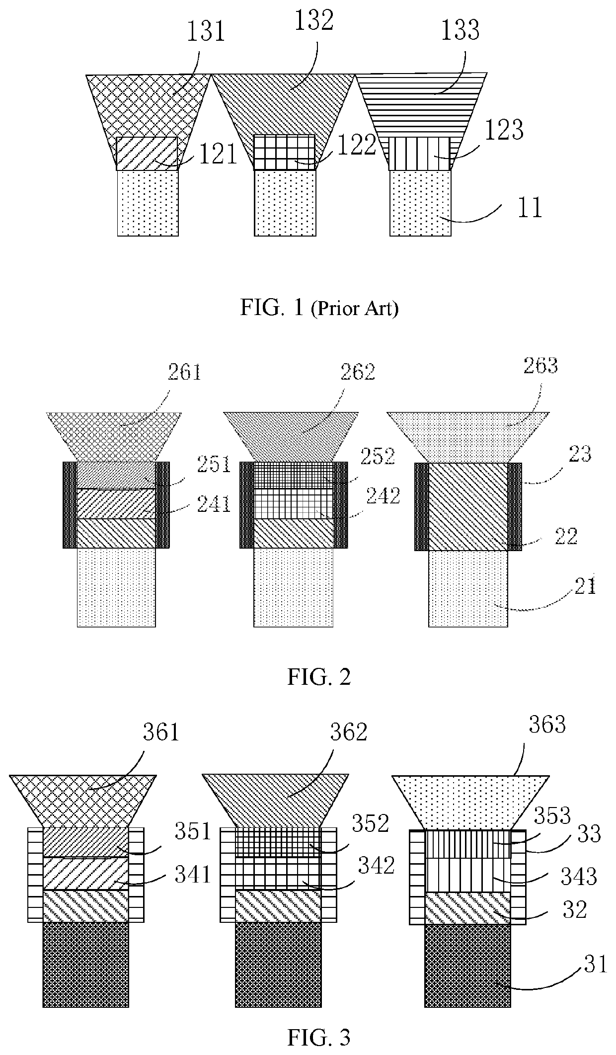
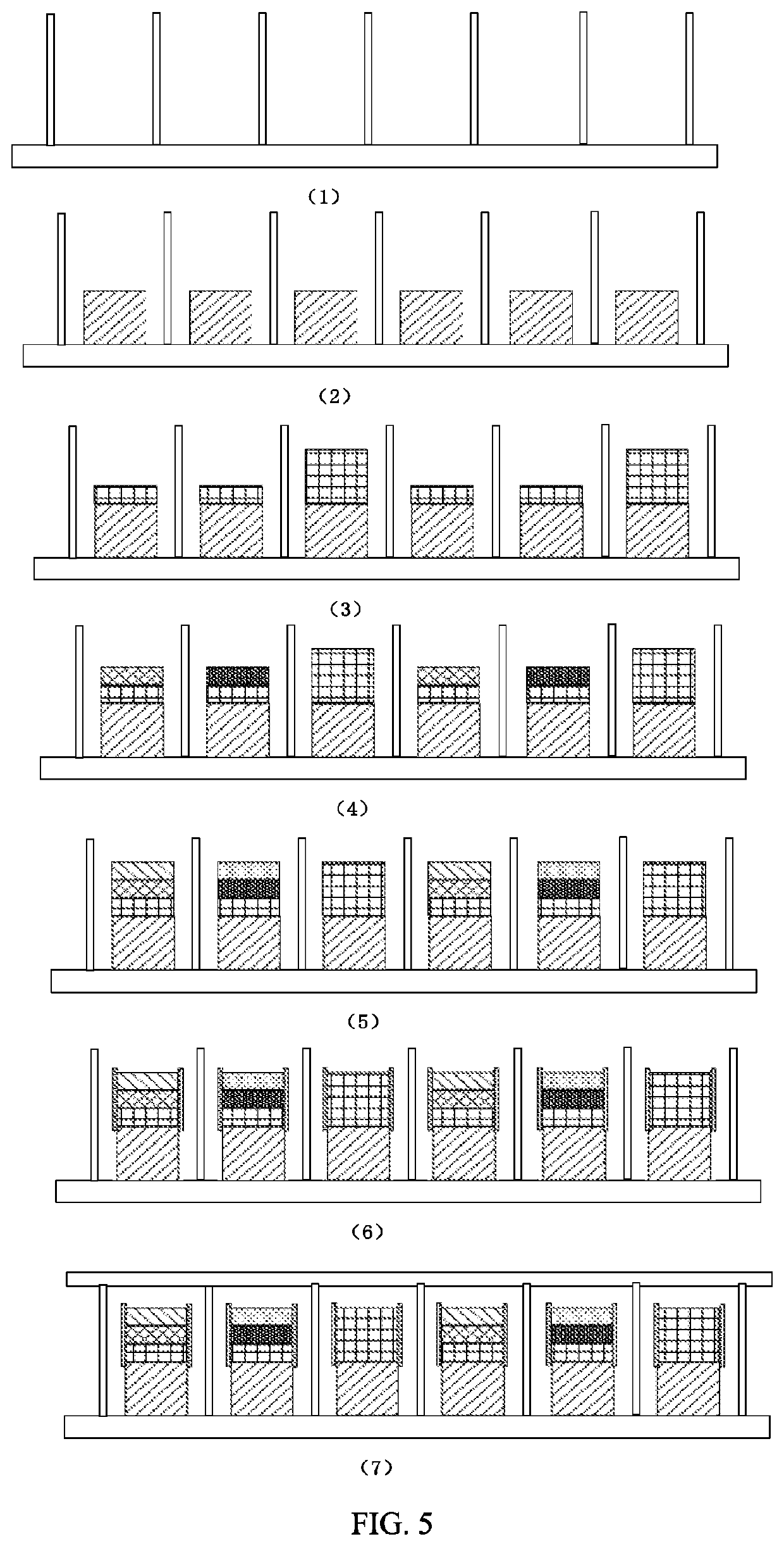
[0037]As shown in FIG. 1, sub-pixel units in a conventional display panel include an excitation light source 11 and a light conversion layer, and the light conversi...


PUM

PropertyMeasurementUnit
thicknessaaaaaaaaaa
transmissionaaaaaaaaaa
light transmissionaaaaaaaaaa

Abstract

The present invention provides a display panel and a method of manufacturing the same. The display panel employs a target light transmission layer disposed on a target light conversion layer for transmitting the target light generated by the target light conversion layer and reflecting the excitation light passing through the target light conversion layer, such that the target light emitted by the sub-pixel units is mixed with a small amount of excitation light or even without excitation light, so that the target light emitted by the sub-pixel units is relatively pure, thereby solving the technical problem that the existing micro-display technology has defects.

Description

BACKGROUND OF INVENTIONField of Invention[0001]The present invention relates to a field of display technology, and in particular, to a display panel and a method of manufacturing the same.Description of Prior Art[0002]Liquid crystal displays (LCDs) and organic light-emitting diode (OLED) displays, as mainstream display devices, each have their own advantages and disadvantages that an LCD has a low light utilization rate and relatively low resolution, while an OLED has a short service life and low brightness. Accordingly, it is needed to develop a display device having better comprehensive effects, such as a quantum dot light emitting diode (QLED), and a mini-light emitting diode (mini-LED), and develop ultimate micro-display technology, such as a micro-light emitting diode (micro-LED).[0003]Micro-LEDs have advantages of high luminous efficiency, low power consumption, high color gamut, a long service life, and good stability. At present, the micro-LEDs are roughly divided into two t...

Claims


Application Information

Patent Timeline
Patent Type & Authority Patents(United States)
IPC IPC(8): H01L27/15H01L33/00H01L33/46H01L33/50
CPCH01L27/156H01L33/0095H01L33/46H01L33/50H01L2933/0041G09F9/33H01L25/0753H01L33/60
Inventor ZHANG, GUIYANGZHA, GUOWEI
Owner WUHAN CHINA STAR OPTOELECTRONICS TECH CO LTD
Why Eureka
Try Eureka