Complex defect diffraction model and method for defect inspection of transparent substrate

a defect inspection and complex defect technology, applied in the field of complex defect inspection models and methods, can solve the problems of inability to detect micro-bubble defects, and inability to completely obtain complex image information of glass substrates, etc., to achieve rapid comparative analysis and high frequency information. the effect of not easy to obtain

Active Publication Date: 2021-04-20
NATIONAL TAIWAN NORMAL UNIVERSITY
View PDF6 Cites 6 Cited by
  • Summary
  • Abstract
  • Description
  • Claims
  • Application Information

AI Technical Summary

Benefits of technology

[0014]The invention utilizes a wide field digital holographic micrography technology to effectively record the diffraction characteristics of bubble, dust, watermark, scratch and other defects and contaminations on a transparent glass substrate, and quantifies and analyses the diffraction characteristics through a machine learning algorithm of defect detection, and detects and classifies the defects to achieve the detection of the transparent glass substrate.

Problems solved by technology

However, in the disclosure of the above-mentioned patent applications, method of detection and classification of defects on glass only performs edge detection for the image to obtain edge information of the defects.
Such methods are not suitable for detection of micro bubble defects on glass, and the micro bubble detection system or device is still needed to be further improved for facilitating detection of the defects.
However, through the machine vision camera, only the intensity image can be obtained, and the complex images information of the glass substrate can't be obtained completely.
Furthermore, it is easy to lose focus or without focusing because the camera can't effectively focus on transparent substrate.
Therefore, it is often necessary to carry out a complicated and time-consuming algorithm for multiple pre-signal processing and classification to proceed the following detection task.
Thus, the existing machine vision can't provide quickly and effectively detect the transparent substrate and improve yield of detection due to the above complicated operations.
That is to say, through machine vision, two-dimensional imaging is not easy and the calculation of image intensity is complex; three-dimensional imaging is time-consuming, and image intensity is dealt with only on a single plane.
This leads to time-consuming of defect detection process, so that only some samples can be extracted to shorten the detection time.
Therefore, how to effectively implement the detection of transparent substrate to improve resolution and field of view, and shorten the detecting time and improve the detection area, has become an important issue in the industry and field of detection.
Therefore, how to improve the field of view and high resolution imaging mechanism to shorten the detection time and increase the number of detection has become an important issue in the current defect detection.
Furthermore, defect detection technology of the traditional industrial products is often not suitable for the penetrating detection of transparent glass substrate.
Then, time-consuming methods of recursive operations are used to obtain hyper-resolution reconstructed images.
Such imaging limitations and time-consuming computational methods are not suitable for defect detection on production lines.
The defects of the transparent substrate may lead to serious yield decline of the whole product process and assembly, and greatly increase the cost of production and waste of resources.
In view of the shortcomings of the above-mentioned technologies, there is no effective and reliable transparent substrate defect detection technology and method available for industrial detection and application in the market at present.

Method used


Image

  • Complex defect diffraction model and method for defect inspection of transparent substrate
  • Complex defect diffraction model and method for defect inspection of transparent substrate
  • Complex defect diffraction model and method for defect inspection of transparent substrate

Examples


Embodiment Construction

[0046]Some preferred embodiments of the present invention will now be described in greater detail. However, it should be recognized that the preferred embodiments of the present invention are provided for illustration rather than limiting the present invention. In addition, the present invention can be practiced in a wide range of other embodiments besides those explicitly described, and the scope of the present invention is not expressly limited except as specified in the accompanying claims.

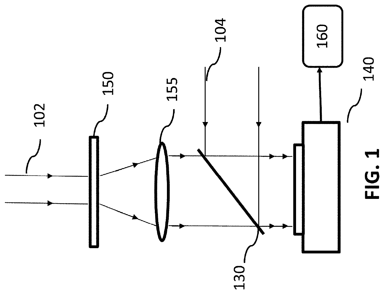
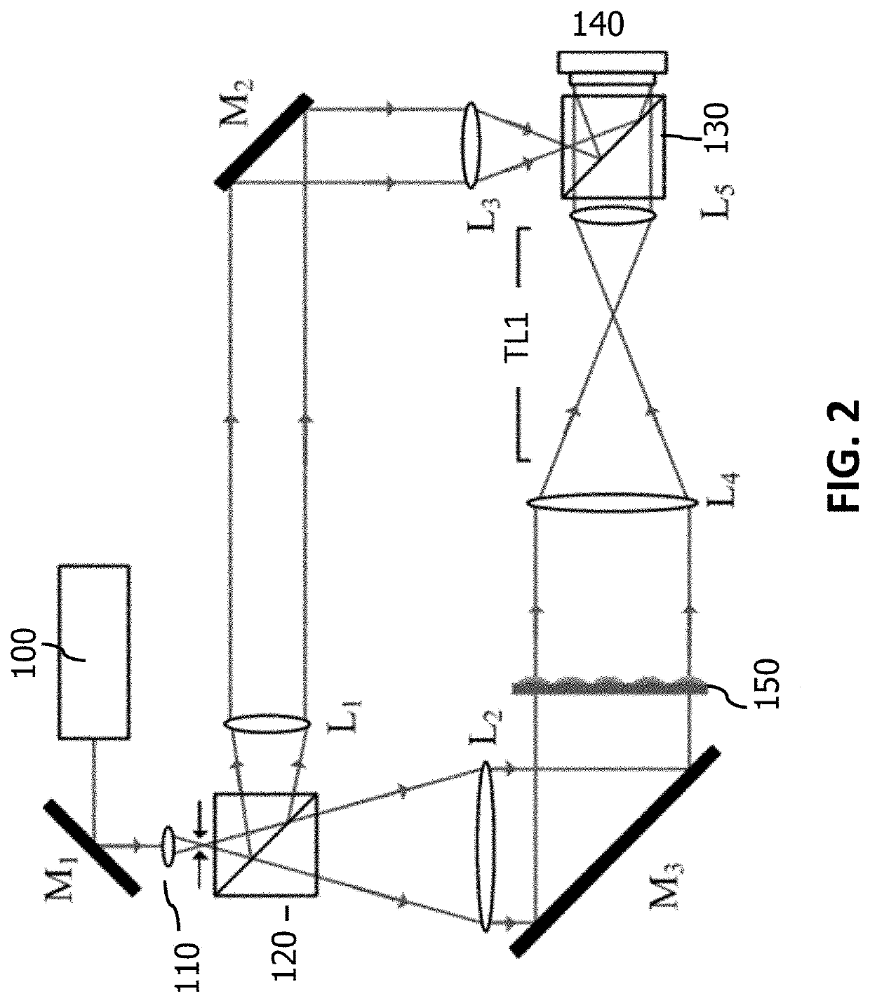
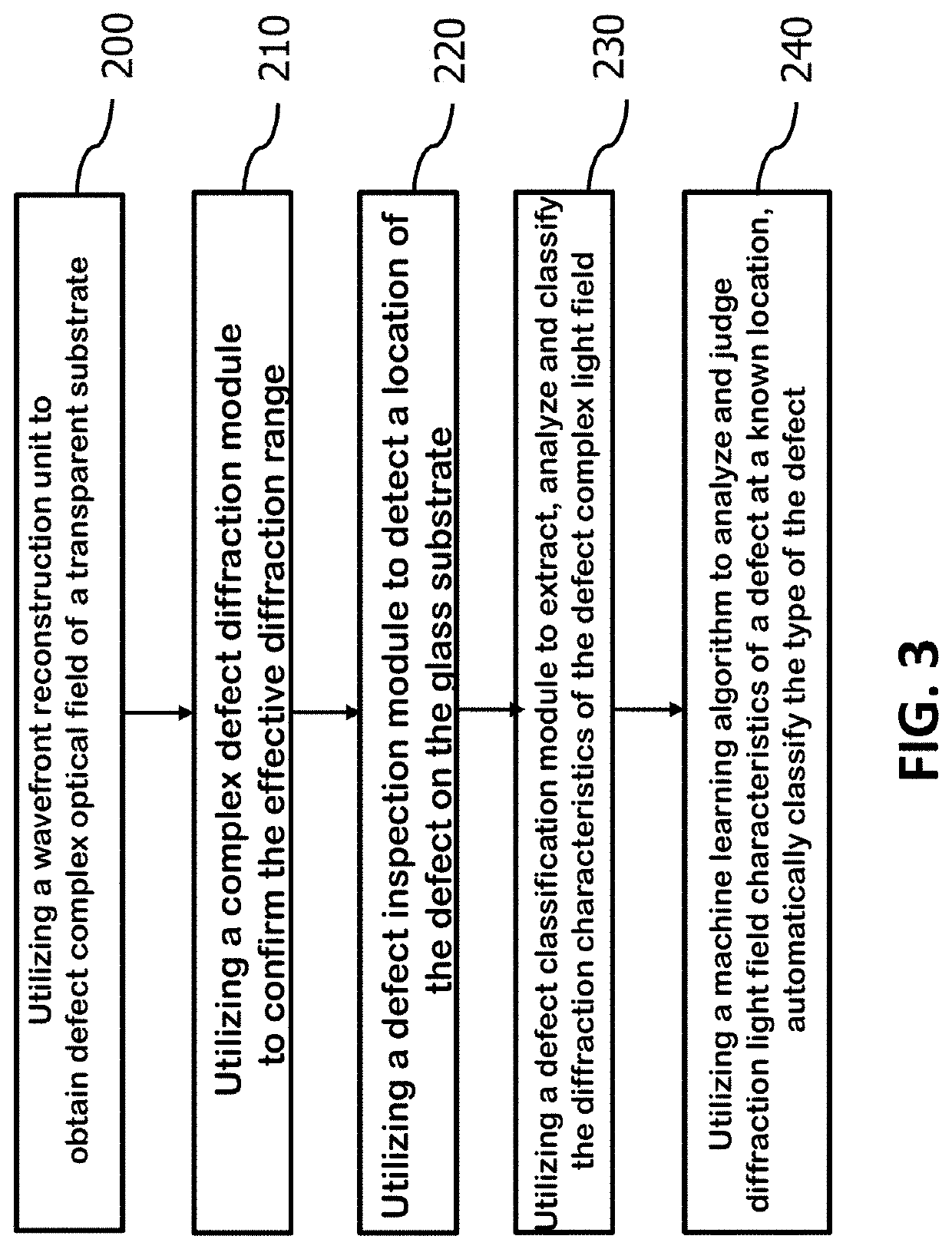
[0047]The proposed digital holography recording method is applied to obtain and record wavefront information of defects on a transparent substrate. Based on this wavefront information, the diffraction fields of defects on different planes are identified and classified through the proposed defect diffraction model. The method of identification and classification is to automatically analyze the wavefront and diffraction characteristics of the defects through computer learning, in order to achieve...


PUM

PropertyMeasurementUnit
focal lengthaaaaaaaaaa
diameteraaaaaaaaaa

Abstract

A method for defect inspection of a transparent substrate comprises utilizing a wavefront reconstruction unit to obtain complex defect diffraction wavefront of a transparent substrate; using a complex defect diffraction module to confirm the effective diffraction distance of the complex defect diffraction wavefront; utilizing a defect detection module to detect position of the defect of the transparent substrate; using a defect classification module to perform extraction, analysis and classification of diffraction characteristics and utilizing a machine learning algorithm or a deep learning algorithm to automatically identify the defects.

Description

TECHNICAL FIELD[0001]The present invention relates to defect inspection of a transparent substrate, and more particularly, to a complex defect diffraction model and method for defect inspection of a transparent substrate.BACKGROUND[0002]Glass substrate is one of the most popular and widely components applied for all kinds of optoelectronic products, such as photoelectric display, intelligent mobile phone panel, micro lens and so on. There are a lot of requirements and applications of glass substrate in the field of optoelectronic industry. Especially, in manufacturing and assembling of photovoltaic products including photoelectric display (for example: liquid crystal display, plasma display panel, organic light emitting diode), digital camera, intelligent mobile phone panel, the glass substrate plays a very significant and key role. In addition, in bonding with silicon chip, microelectromechanical systems (MEMS), Bio-medical, micro mirror, micro glass-block, polarized beam splitter,...

Claims


Application Information

Patent Timeline
Patent Type & Authority Patents(United States)
IPC IPC(8): G03H1/00G03H1/04G01N21/958
CPCG03H1/0443G01N21/958G03H1/0005G03H1/0465G03H2001/005G03H2001/0445G03H2001/0452G01N2021/8967G03H1/0866G03H2001/0883
Inventor CHENG, CHAU-JERNTU, HAN-YENCHANG CHIEN, KUANG-CHELIN, YU-CHIH
Owner NATIONAL TAIWAN NORMAL UNIVERSITY
Why Eureka
Try Eureka