Pixel compensation circuit and OLED display device

a compensation circuit and display device technology, applied in the field of display, can solve the problems of uneven brightness of the entire oled display device, deformation of the pixel compensation circuit, and drifting threshold voltage of the tft, and achieve the effect of improving ppi and high ppi

Active Publication Date: 2021-04-20
WUHAN CHINA STAR OPTOELECTRONICS SEMICON DISPLAY TECH CO LTD
View PDF12 Cites 0 Cited by
  • Summary
  • Abstract
  • Description
  • Claims
  • Application Information

AI Technical Summary

Benefits of technology

[0010]An object of the present disclosure is to provide a pixel compensation circuit and an organic light-emitting diode (OLED) display device to deal with the problems of the related art as mentioned above. The adoption of the pixel compensation circuit and the OLED display device is good for reducing the space of the pixel structure, increase the pixel density, and facilitate the design of a panel with high pixels per inch (PPI).
[0014]The advantage of the present disclosure is as follows: Two or more TFTs are controlled by the scanning signal output from the scanning signal line in the same row in the pixel compensation circuit proposed by the present disclosure. Further, the OLED and the storage capacitor are both connected to the reset voltage signal line. So the OLED and the storage capacitor are reset after receiving the reset voltage signal. Each of the TFTs is of a single-gate structure. Or, one or more of the TFTs is of a double-gate or a multi-gate structure. The TFTs share one or more portion of the active layer. At the same time, the polysilicon traces for the active layers of the two TFTs are only two in the vertical direction, thereby compressing the size of the pixel structure in the horizontal direction, providing space for the improvement of the PPI, and facilitating the design a panel with high PPI.

Problems solved by technology

Especially, a threshold voltage of the TFT often drifts.
The stability is degraded after the bias is turned on for a long time.
The brightness of the entire OLED display device is uneven.

Method used


Image

  • Pixel compensation circuit and OLED display device
  • Pixel compensation circuit and OLED display device
  • Pixel compensation circuit and OLED display device

Examples


Embodiment Construction

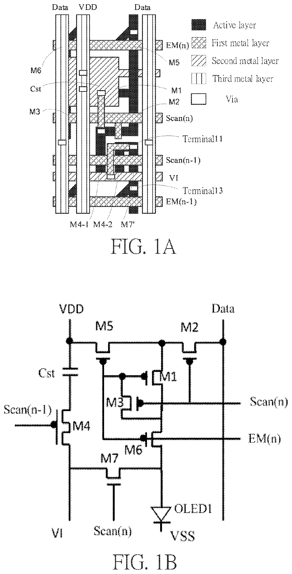
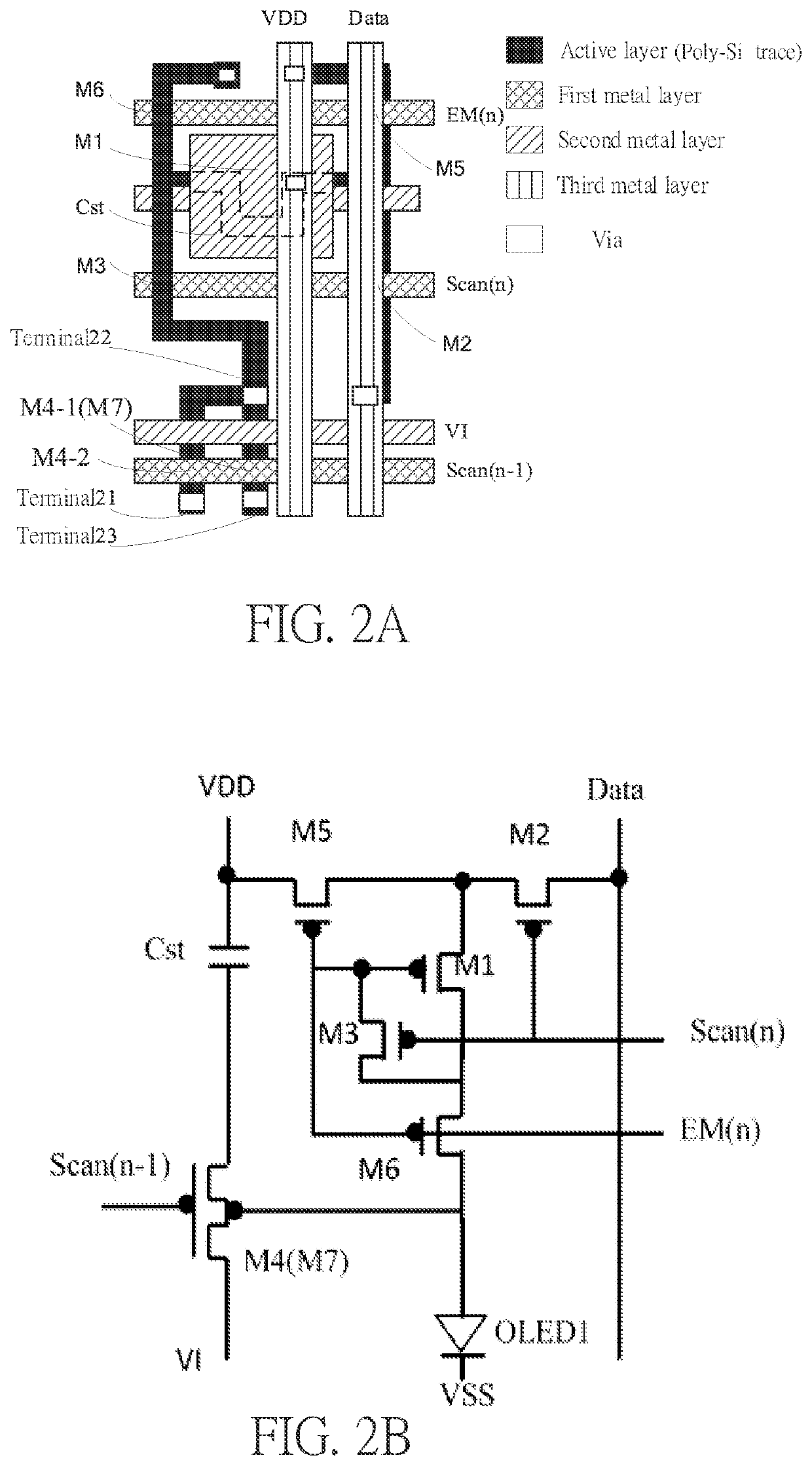
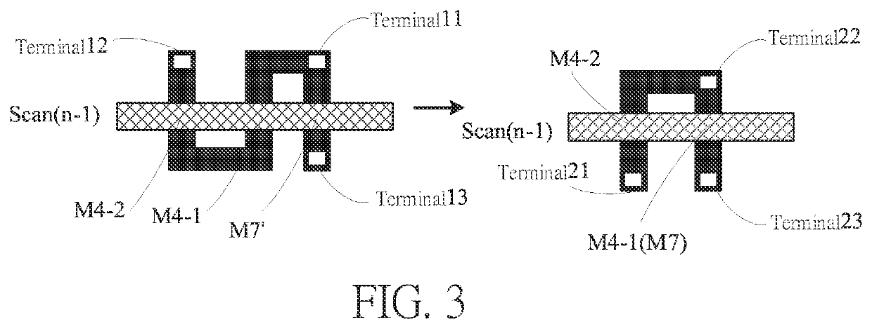
[0021]The invention is described below in detail with reference to the accompanying drawings, wherein like reference numerals are used to identify like elements illustrated in one or more of the figures thereof, and in which exemplary embodiments of the invention are shown. This invention may, however, be embodied in many different forms and should not be construed as limited to the particular embodiments set forth herein. Rather, these embodiments are provided so that this disclosure will be thorough and complete, and will fully convey the scope of the invention to those skilled in the art.

[0022]It should further be understood that, although the terms first, second, third, and the like may be used herein to describe various elements, components, regions, layers and / or sections, these elements, components, regions, layers and / or sections should not be limited by these terms. These terms are used only to distinguish one element, component, region, layer or section from another region...


PUM

PropertyMeasurementUnit
reset voltageaaaaaaaaaa
driving voltageaaaaaaaaaa
voltageaaaaaaaaaa

Abstract

A pixel compensation circuit and an OLED display device are disclosed. Two or more TFTs are controlled by the scanning signal output from the scanning signal line in the same row in the pixel compensation circuit proposed by the present disclosure. Further, the OLED and the storage capacitor are both connected to the reset voltage signal line. So the OLED and the storage capacitor are reset after receiving the reset voltage signal. The size of the pixel structure in the horizontal direction is compressed in the pixel compensation circuit of the present disclosure, thereby providing space for the improvement of the PPI and facilitating the design of the high PPI panel successfully.

Description

RELATED APPLICATIONS[0001]This application is a National Phase of PCT Patent Application No. PCT / CN2019 / 095073 having International filing date of Jul. 8, 2019, which claims the benefit of priority of Chinese Patent Application No. 201910396424.7 filed on May 14, 2019. The contents of the above applications are all incorporated by reference as if fully set forth herein in their entirety.FIELD AND BACKGROUND OF THE INVENTION[0002]The present disclosure relates to the field of display, and more particularly, to a pixel compensation circuit and an organic light-emitting diode (OLED) display device.[0003]The rapid development of organic light emitting diode (OLED) display technology has promoted the rapid entry of curved surface and flexible display products into the market in recent years. The technological update in related fields is also changing with each passing day. OLED refers to a diode that emits light by carrier injection and recombination under the electric field driven by an...

Claims


Application Information

Patent Timeline
Patent Type & Authority Patents(United States)
IPC IPC(8): G09G3/3266G09G3/3258G09G3/3275H01L27/32
CPCG09G3/3266G09G3/3258G09G3/3275H01L27/3262H01L27/3265H01L27/3276G09G2300/0465G09G3/325G09G2300/0426H10K59/131H10K59/1213H10K59/1216
Inventor WANG, WEIXU, PINQUAN
Owner WUHAN CHINA STAR OPTOELECTRONICS SEMICON DISPLAY TECH CO LTD
Why Eureka
Try Eureka