TFT pixel threshold voltage compensation circuit with data programming from drain of the drive TFT

a technology of data programming and threshold voltage, applied in the direction of instruments, static indicating devices, etc., can solve the problems of residual voltage affecting the true black state, pixel brightness may not be uniform for a given vdat value, and performance degradation by memory effects from previous frame data, so as to achieve less impact on performance

Active Publication Date: 2021-06-29
SHARP KK
View PDF5 Cites 0 Cited by
  • Summary
  • Abstract
  • Description
  • Claims
  • Application Information

AI Technical Summary

Benefits of technology

[0012]The present application relates to pixel circuits that are capable of compensating the threshold voltage variations of the drive transistor. In embodiments of the present application, in contrast to conventional configurations, data programming is performed using the drain of the drive transistor rather than the gate or source of the drive transistor as is typical. A benefit of data programming from the drain side of the drive transistor is that this architecture removes a separate initialization voltage supply line. As the data is programmed one row at a time, and one column data voltage only supplies one pixel, the IR drop has substantially less impact on performance than using a separate initialization voltage as done in conventional configurations.
[0013]An aspect of the invention, therefore, is a pixel circuit for a display device that provides enhanced performance by performing drain-side initialization and data programming with respect to the drive transistor. In exemplary embodiments, the pixel circuit is operable in an initialization phase, a combined threshold compensation and data programming phase, and an emission phase, the pixel circuit including a drive transistor configured to control an amount of current to a light-emitting device during the emission phase depending upon a voltage applied to a gate of the drive transistor, the drive transistor having a first terminal and a second terminal with the first terminal being electrically connected during the emission phase to a first voltage supply line that supplies a driving voltage; a capacitor having a first plate that is electrically connected to the gate of the drive transistor during the emission phase and a second plate connected to the first terminal of the drive transistor; and a light-emitting device that is electrically connected at a first terminal to the second terminal of the drive transistor during the emission phase and is connected at a second terminal to a second voltage supply line. The second terminal of the drive transistor is electrically connected to a data voltage supply line that supplies a data voltage during the initialization phase and the combined threshold compensation and data programming phase to compensate a threshold voltage of the drive transistor and to program the data voltage.
[0015]Another aspect of the invention is a method of operating a pixel circuit in a manner that provides enhanced performance by performing drain-side initialization and data programming with respect to the drive transistor. In exemplary embodiments, the method of operating includes the steps of providing a pixel circuit in accordance with any of the embodiments; performing an initialization phase to initialize voltages within the pixel circuit and performing a combined threshold compensation and data programming phase to compensate a threshold voltage of the drive transistor and to program a data voltage, each of the initialization phase and the combined threshold compensation and data programming phase comprising: diode-connecting the drive transistor by electrically connecting a gate and the second terminal of the drive transistor; and electrically connecting the second terminal of the drive transistor to a data voltage supply line that supplies the data voltage to apply the data voltage to the second terminal of the drive transistor; and performing an emission phase during which light is emitted from the light-emitting device comprising: electrically connecting the first terminal of the drive transistor and the first power supply line; electrically connecting the gate of the drive transistor and the first plate of the capacitor; and electrically connecting the first terminal of the light-emitting device and the second terminal of the drive transistor to apply the driving voltage from the first voltage supply line to the light-emitting device through the drive transistor. In exemplary embodiments, the initialization phase further may include electrically disconnecting the first terminal of the light-emitting device from the first voltage supply line, and electrically connecting the first terminal of the light-emitting device to the data voltage supply line to apply the data voltage to the first terminal of the light-emitting device.

Problems solved by technology

Therefore, pixels in a display may not exhibit uniform brightness for a given VDAT value.
A first problem with this is that the residual voltage may affect the true black state.
A second problem is degradation of performance by memory effects from the previous frame data.
If the programmed current for the current frame is a relatively low current, it could take a significant time to refresh the anode to the programmed value.
However, the initialization voltage supplies at least one row, and there could thousands of pixels in one row and thus a large current draw stems from the initialization voltage.
With this configuration, the positive power supply and the negative power supply have to change to the opposite power levels for initializing the pixel circuit, and this may consume more power.
This configuration employs multiple levels for the positive power supply, and thus may consume more power.

Method used


Image

  • TFT pixel threshold voltage compensation circuit with data programming from drain of the drive TFT
  • TFT pixel threshold voltage compensation circuit with data programming from drain of the drive TFT
  • TFT pixel threshold voltage compensation circuit with data programming from drain of the drive TFT

Examples


first embodiment

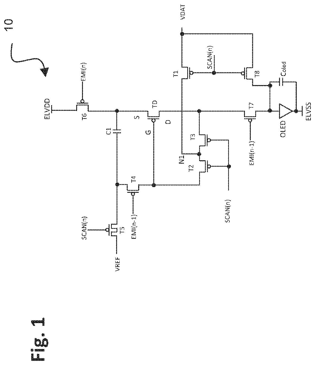
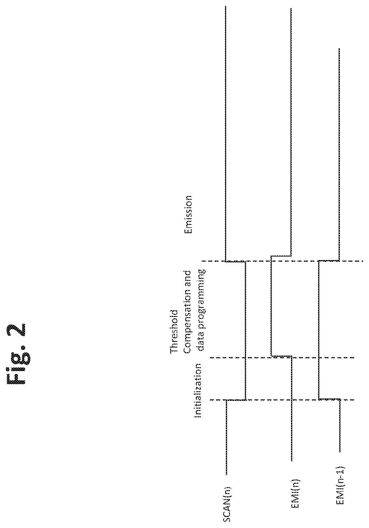
[0029]As illustrated in the timing diagram of FIG. 2, in this first embodiment, during the previous emission phase the EMI(n) and EMI(n−1) signal levels have a low voltage value, so transistors T4, T6, and T7 are in an on state, and light emission is being driven by the input driving voltage ELVDD connected by a power supply line to the drive transistor TD, whereby the actual current applied to the OLED is determined by the voltage at the gate and the source of the drive transistor. The SCAN(n) signal levels for the applicable rows initially have a high voltage value so switch transistors T1, T2, T3, T5, and T8 are in an off state.

[0030]At the beginning of the initialization phase, the EMI(n−1) signal level is changed from a low voltage level to a high voltage level, causing the transistors T4 and T7 to be placed in the off state. The capacitor C1 has a first plate connected to switch transistors T4 and T5, and a second plate connected to a first terminal or source of the drive tran...

second embodiment

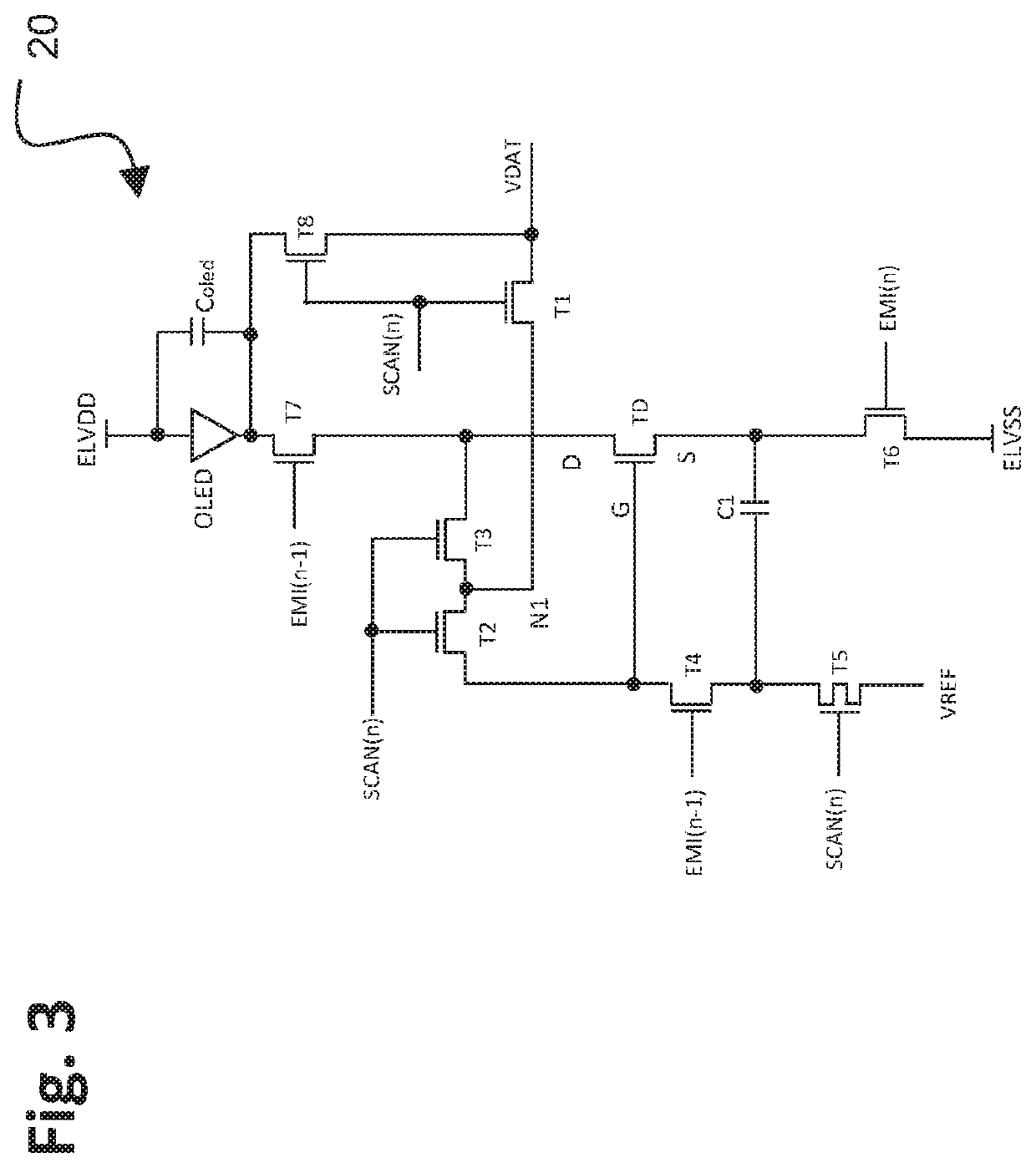
[0044]The control signal levels depicted in the timing diagram of FIG. 4 are basically comparable to the control signal levels depicted in the timing diagram of FIG. 2, except modified as warranted for the operation of n-type transistors rather than p-type transistors. In this second embodiment, during the previous emission phase, the EMI(n) and EMI(n−1) signal levels have a high voltage value, so transistors T4, T6, and T7 are in an on state, and light emission is being driven by the input driving voltage ELVSS connected to the drive transistor TD, whereby the actual current applied to the OLED is determined by the voltage at the gate and the source of the drive transistor. The SCAN(n) signal levels for the applicable rows initially have a low voltage value so transistors T1, T2, T3, T5, and T8 are in an off state.

[0045]Referring to the TFT circuit 20 of FIG. 3 in combination with the timing diagram of FIG. 4, similarly as the previous embodiment the TFT circuit 20 operates to perf...


PUM


Abstract

A pixel circuit for a display device provides enhanced performance by performing drain-side initialization and data programming with respect to the drive transistor. The pixel circuit is operable in an initialization phase, a combined threshold compensation and data programming phase, and an emission phase, the pixel circuit including a drive transistor configured to control an amount of current to a light-emitting device during the emission phase depending upon a voltage applied to a gate of the drive transistor, and the drive transistor having a first terminal and a second terminal with the first terminal being electrically connected during the emission phase to a first voltage supply line that supplies a driving voltage. The second terminal of the drive transistor is electrically connected to a data voltage supply line that supplies a data voltage during the initialization phase and the combined threshold compensation and data programming phase to compensate a threshold voltage of the drive transistor and to program the data voltage.

Description

TECHNICAL FIELD[0001]The present application relates to design and operation of electronic circuits for delivering electrical current to an element in a display device, such as for example to an organic light-emitting diode (OLED) in the pixel of an active matrix OLED (AMOLED) display device.BACKGROUND ART[0002]Organic light-emitting diodes (OLED) generate light by re-combination of electrons and holes, and emit light when a bias is applied between the anode and cathode such that an electrical current passes between them. The brightness of the light is related to the amount of the current. If there is no current, there will be no light emission, so OLED technology is a type of technology capable of absolute blacks and achieving almost “infinite” contrast ratio between pixels when used in display applications.[0003]Several approaches are taught in the prior art for pixel thin film transistor (TFT) circuits to deliver current to an element of a display device, such as for example an o...

Claims


Application Information

Patent Timeline
Patent Type & Authority Patents(United States)
IPC IPC(8): G09G3/3233G09G3/3266G09G3/3291
CPCG09G3/3233G09G3/3266G09G3/3291G09G2300/0814G09G2300/0819G09G2300/0866G09G2310/08G09G2320/045
Inventor LU, TONG
Owner SHARP KK
Why Eureka
Try Eureka