Elastic wave device and method of manufacturing the same

a technology of elastic wave and manufacturing method, which is applied in the direction of piezoelectric/electrostrictive/magnetostrictive devices, electrical apparatus, impedence networks, etc., can solve the problems of failure of inspection electrode and terminal electrode contact, poor degree of parallelism between the upper surface of sealing resin and the lower surface of the mounting substrate, and failure of inspection electrode and the terminal electrod

Active Publication Date: 2021-10-26
MURATA MFG CO LTD
View PDF12 Cites 0 Cited by
  • Summary
  • Abstract
  • Description
  • Claims
  • Application Information

AI Technical Summary

Benefits of technology

[0007]Preferred embodiments of the present invention provide elastic wave devices in which a degree of parallelism between an upper surface of a sealing resin and a terminal electrode is good and in which a failure in contact between the terminal electrode on a mounting substrate and an inspection electrode is unlikely to occur.

Problems solved by technology

In fact, however, many mounting substrates have non-uniform thicknesses for various reasons.
In the case where the elastic wave element is mounted above such a mounting substrate and then sealed with a resin, the degree of parallelism between the upper surface of a sealing resin and the lower surface of the mounting substrate and between the upper surface of the sealing resin and a terminal electrode may not be good.
Accordingly, a failure in contact between an inspection electrode and the terminal electrode may occur in an inspecting process.

Method used


Image

  • Elastic wave device and method of manufacturing the same
  • Elastic wave device and method of manufacturing the same
  • Elastic wave device and method of manufacturing the same

Examples


Embodiment Construction

[0027]Preferred embodiments of the present invention will hereinafter be described in detail with reference to the drawings to clarify the present invention.

[0028]The preferred embodiments are described by way of example in the present disclosure. The features of various preferred embodiments of the present invention can be partially replaced or combined.

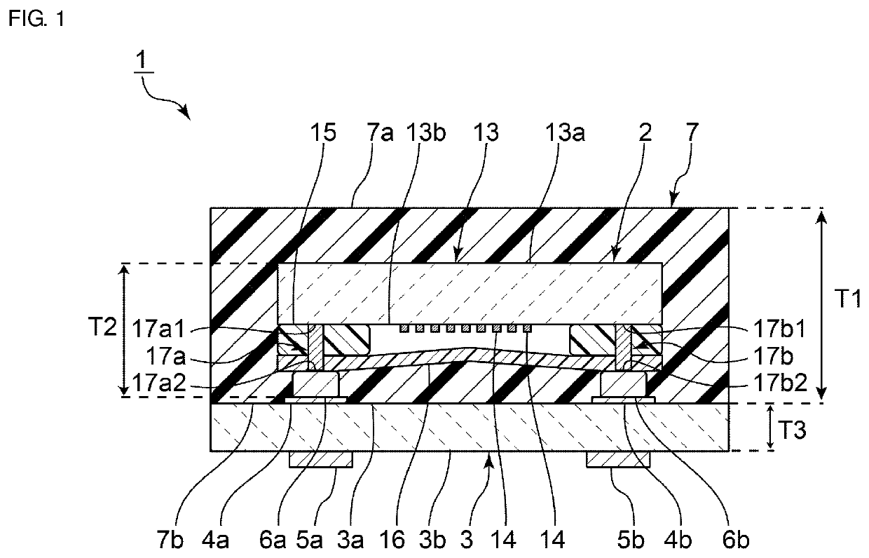
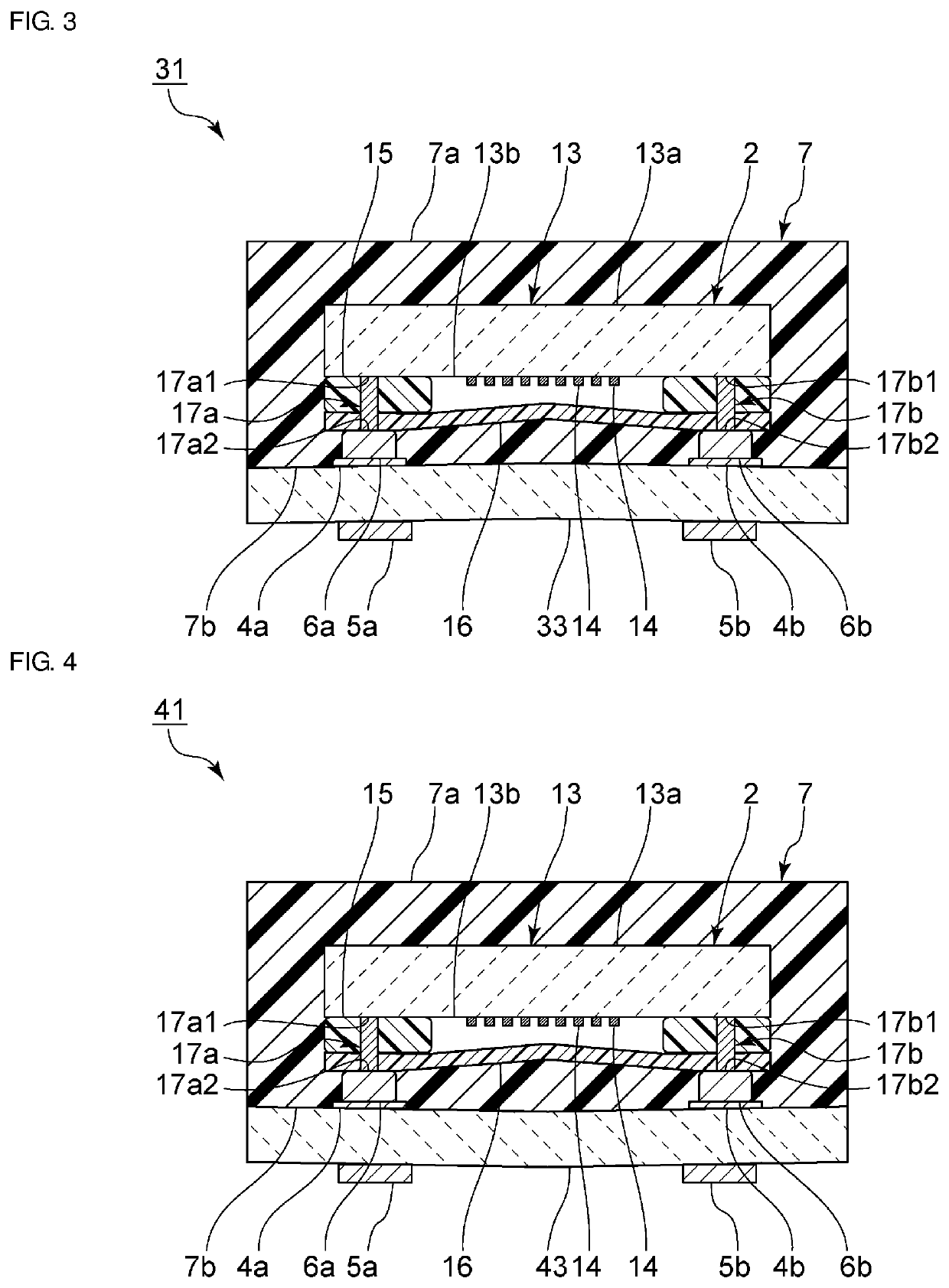
[0029]FIG. 1 is a front sectional view of an elastic wave device according to a first preferred embodiment of the present invention.

[0030]An elastic wave device 1 includes a mounting substrate 3. The mounting substrate 3 includes an upper surface 3a and a lower surface 3b that face each other. The material of the mounting substrate 3 is not particularly limited and may be, for example, a proper ceramic, or a resin including a glass epoxy resin.

[0031]Electrode lands 4a and 4b are disposed on the upper surface 3a of the mounting substrate 3. Terminal electrodes 5a and 5b to be electrically connected to the outside are disposed on the ...


PUM

PropertyMeasurementUnit
thicknessaaaaaaaaaa
thicknessaaaaaaaaaa
thicknessaaaaaaaaaa

Abstract

An elastic wave device includes an elastic wave element including a piezoelectric substrate with a first main surface and a second main surface that face each other, an IDT electrode disposed on the second main surface of the piezoelectric substrate, a support disposed on the second main surface of the piezoelectric substrate so as to surround the IDT electrode in plan view, and a cover that is disposed on the support and seals the IDT electrode together with the support and the piezoelectric substrate, a mounting substrate above which the elastic wave element is mounted, and a sealing resin that is disposed on the side of the side of the upper surface of the mounting substrate and seals the elastic wave element. A thickness of the mounting substrate is less than a thickness of the sealing resin that corresponds to a distance from a surface of the sealing resin in contact with the upper surface of the mounting substrate to a surface of the sealing resin on an opposite side of the mounting substrate.

Description

CROSS REFERENCE TO RELATED APPLICATIONS[0001]This application claims the benefit of priority to Japanese Patent Application No. 2015-051813 filed on Mar. 16, 2015 and is a Continuation Application of PCT Application No. PCT / JP2016 / 055244 filed on Feb. 23, 2016. The entire contents of each application are hereby incorporated herein by reference.BACKGROUND OF THE PRESENT INVENTION1. Field of the Invention[0002]The present invention relates to an elastic wave device including an elastic wave element with a WLP (Wafer Level Package) structure that is mounted above a mounting substrate.2. Description of the Related Art[0003]Conventionally, elastic wave devices each including an elastic wave element having a WLP structure that is mounted above a mounting substrate are in widespread use in, for example, cellular phones.[0004]In an elastic wave device disclosed in Japanese Unexamined Patent Application Publication No. 2010-278971, an elastic wave element above a mounting substrate is sealed...

Claims


Application Information

Patent Timeline
Patent Type & Authority Patents(United States)
IPC IPC(8): H03H9/25H01L41/053H03H9/02H03H3/08H03H9/10H03H9/05
CPCH03H9/0222H03H3/08H03H9/059H03H9/1071H03H9/25
Inventor KOREEDA, TOSHISHIGESUMII, HIJIRI
Owner MURATA MFG CO LTD
Why Eureka
Try Eureka