System for link management between multiple communication chips

a communication chip and link management technology, applied in the field of coordinating operations of multiple integrated circuits (ic) chips, can solve problems such as resource usage collision, interference in shared or overlapping communication bands, and possible complications

Active Publication Date: 2021-11-16
APPLE INC
View PDF7 Cites 5 Cited by
  • Summary
  • Abstract
  • Description
  • Claims
  • Application Information

AI Technical Summary

Problems solved by technology

As a result of integrating multiple communication systems and other subsystems in the electronic device, various issues or complications may arise.
These issues or complications include, among others, collision in terms of resource usage, interference in shared or overlapping communication bands, mutually incompatible modes of operations, isolation between antennas, and transmit power management among various concurrently active SOCs.

Method used


Image

  • System for link management between multiple communication chips
  • System for link management between multiple communication chips
  • System for link management between multiple communication chips

Examples


example electronic

Device

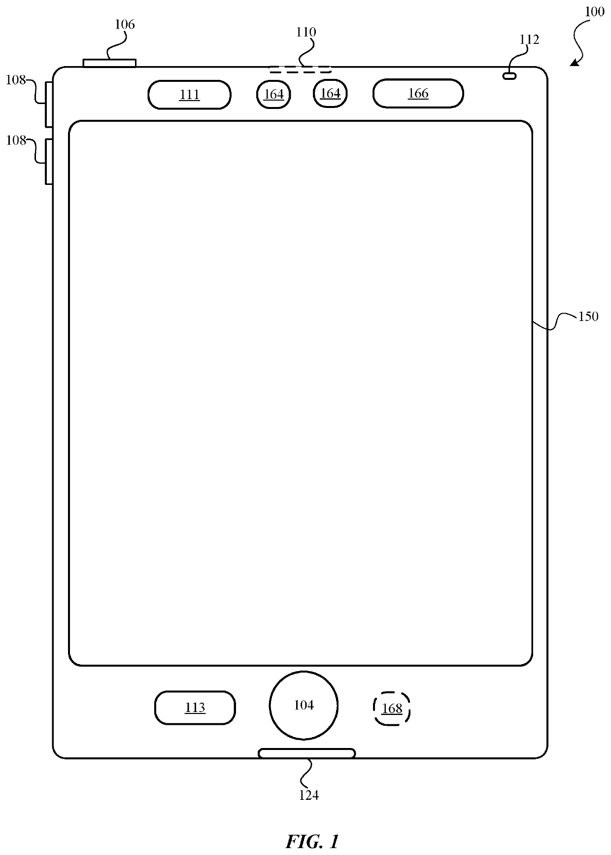
[0021]Embodiments of electronic devices, user interfaces for such devices, and associated processes for using such devices are described. In some embodiments, the device is a portable communications device, such as a mobile telephone, that also contains other functions, such as personal digital assistant (PDA) and / or music player functions. Exemplary embodiments of portable multifunction devices include, without limitation, the iPhone®, iPod Touch®, Apple Watch®, and iPad® devices from Apple Inc. of Cupertino, Calif. Other portable electronic devices, such as wearables, laptops or tablet computers, are optionally used. In some embodiments, the device is not a portable communications device, but is a desktop computer or other computing device that is not designed for portable use. In some embodiments, the disclosed electronic device may include a touch sensitive surface (e.g., a touch screen display and / or a touch pad). An example electronic device described below in conjunctio...

example communication

System in Electronic Device

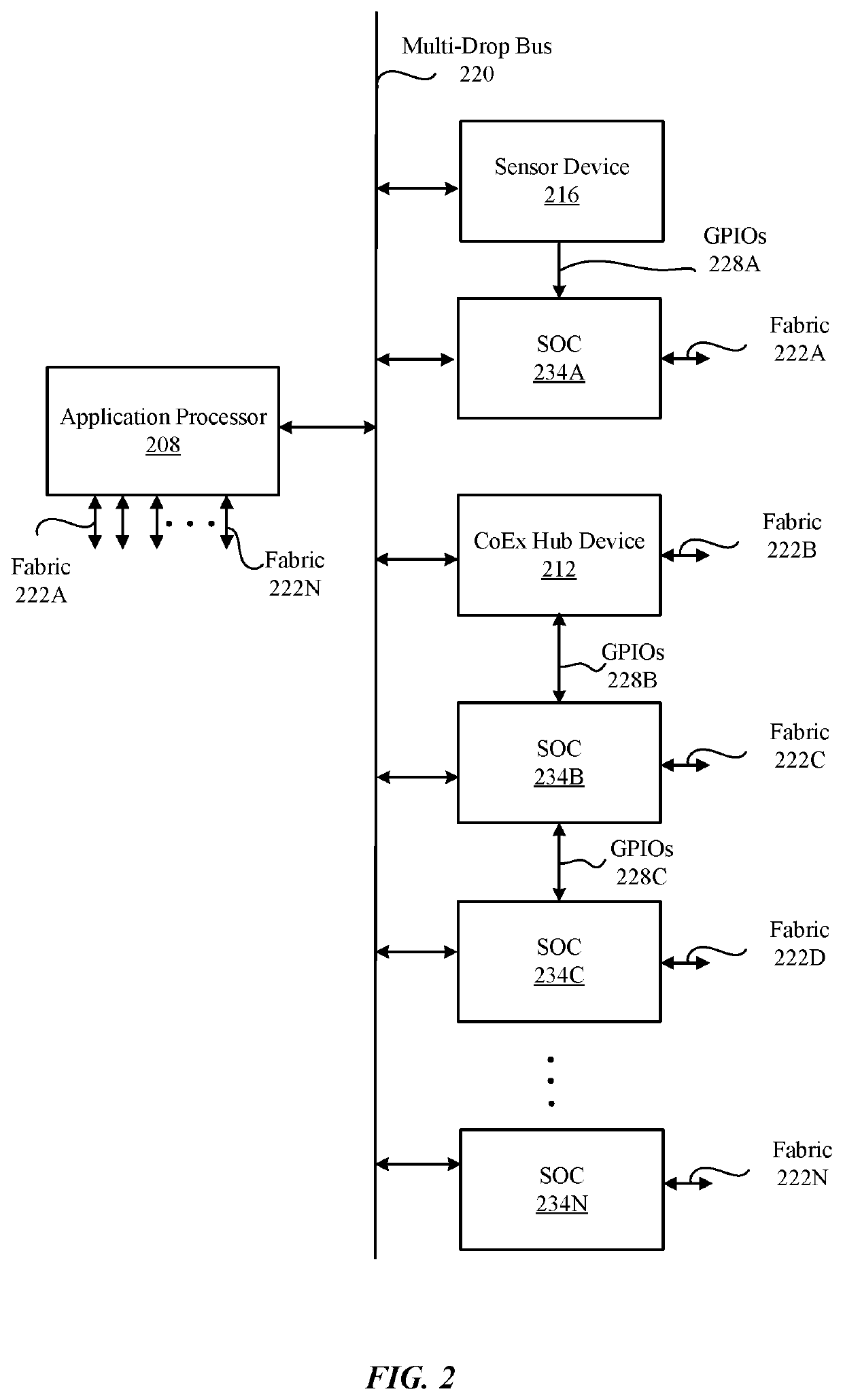
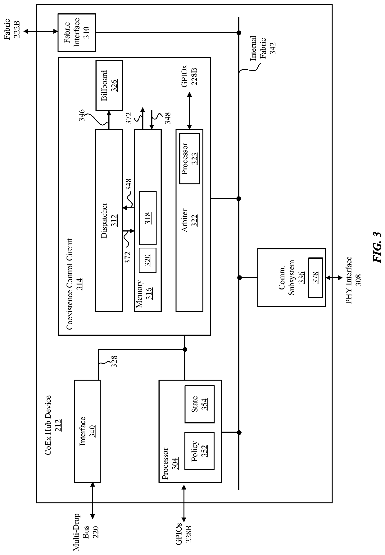
[0025]FIG. 2 is a block diagram illustrating components of electronic device 100 communicating over a multi-drop bus 220, according to one embodiment. Electronic device 100 may include, among other components, an application processor 208 (also referred to as “a central processor” herein), a coexistence hub device 212 (also referred to as “a coexistence hub device” herein), SOCs 234A through 234N (collectively referred to as “SOCs 234” herein), a sensor device 216, multi-drop bus 220, and fabrics 222A through 222N (collectively referred to as “fabrics 222” herein). The components illustrated in FIG. 2 may be part of a communication subsystem in electronic device 100. Electronic device 100 may include additional components (e.g., user interfaces) not illustrated in FIG. 2.

[0026]Application processor 208 is a processing circuit in electronic device 100 for executing various operations. Application processor 208 may include one or more processing cores for ex...


PUM


Abstract

Embodiments relate to an integrated circuit of an electronic device that coordinates activities with another integrated circuit of the electronic device. The integrated circuit includes an interface circuit and a processor circuit. The interface circuit communicates over a multi-drop bus connected to multiple electronic components. The processor circuit receives an authorization request from the integrated circuit via the interface circuit and the multi-drop bus. The received authorization request relates to authorization to perform an activity on the other integrated circuit. In response to receiving the authorization request, the processor circuit determines whether the other integrated circuit is authorized to execute the activity. In response to determining that the other integrated circuit is authorized to execute the activity, the processor circuit sends, to the other integrated circuit over a configurable direct connection, an authorization signal authorizing the other integrated circuit to execute the activity.

Description

CROSS REFERENCE TO RELATED APPLICATIONS[0001]This application claims benefit of U.S. Provisional Patent Application Ser. No. 62 / 957,048, filed Jan. 3, 2020, which is hereby incorporated by reference in its entirety.BACKGROUND1. Field of the Disclosure[0002]The present disclosure relates to coordinating operations of multiple integrated circuit (IC) chips in an electronic device.2. Description of the Related Art[0003]Electronic devices may include multiple systems on chips (SOCs) for communicating with other devices using various communication protocols. As the size of a communication system in an electronic device becomes smaller while the functionality of the communication system increases, more SOCs are incorporated into the electronic device or more subsystems are added to each SOC. These SOCs may communicate with a host (e.g., a central processor or an application processor) over a dedicated communication path (e.g., peripheral component interconnect express (PCIe)) to transmit ...

Claims


Application Information

Patent Timeline
Patent Type & Authority Patents(United States)
IPC IPC(8): G06F13/362G06F13/24G06F11/34G06F11/30G06F13/28
CPCG06F13/3625G06F11/3051G06F11/3409G06F13/24G06F13/28G06F2213/0038G06F9/5011G06F13/12G06F11/3055G06F13/4068G06F2213/40
Inventor O'SHEA, HELENA DEIRDRECHEN, CAMILLERAMAMURTHI, VIJAY KUMARPAYCHER, ALONSAUER, MATTHIASADLER, BERND W.
Owner APPLE INC
Why Eureka
Try Eureka