Supercharge Your Innovation With Domain-Expert AI Agents!

Imaging device and imaging system

a technology of imaging system and imaging device, which is applied in the field of imaging device and imaging system, can solve problems such as deterioration of af performance, and achieve the effect of fast image capture and af performan

Active Publication Date: 2021-12-14
CANON KK
View PDF32 Cites 2 Cited by
  • Summary
  • Abstract
  • Description
  • Claims
  • Application Information

AI Technical Summary

Benefits of technology

The present invention is an imaging device that can capture images faster and more easily regardless of the number of rows that have simultaneous AD conversion. This device also has improved AF performance.

Problems solved by technology

In recent years, the number of rows on which AD conversion is simultaneously performed has increased in accordance with a demand for faster sensors, and there is a concern of deterioration of AF performance in the scheme in Japanese Patent Application Laid-open No. 2019-047267.

Method used


Image

  • Imaging device and imaging system
  • Imaging device and imaging system
  • Imaging device and imaging system

Examples


first embodiment

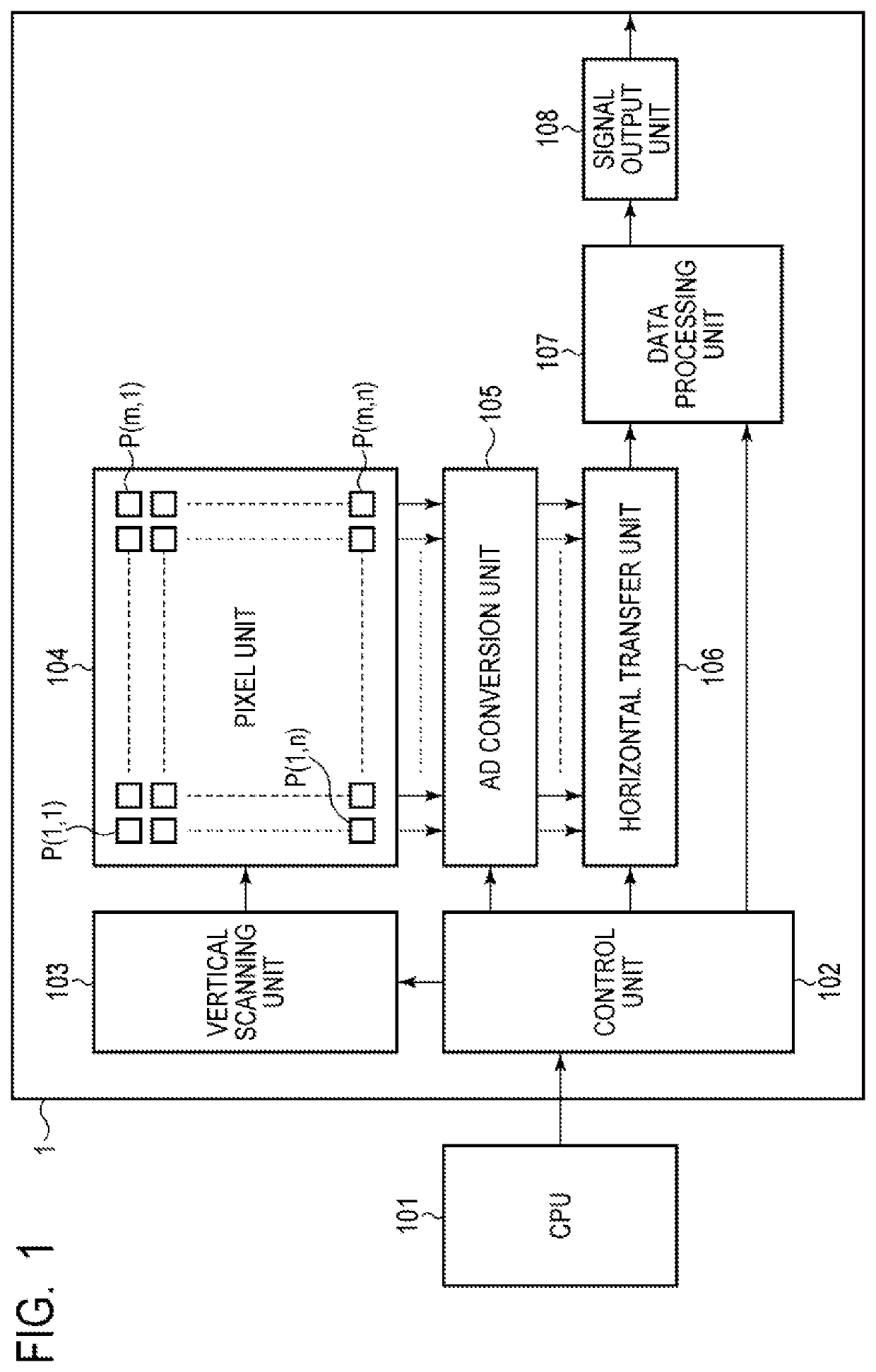
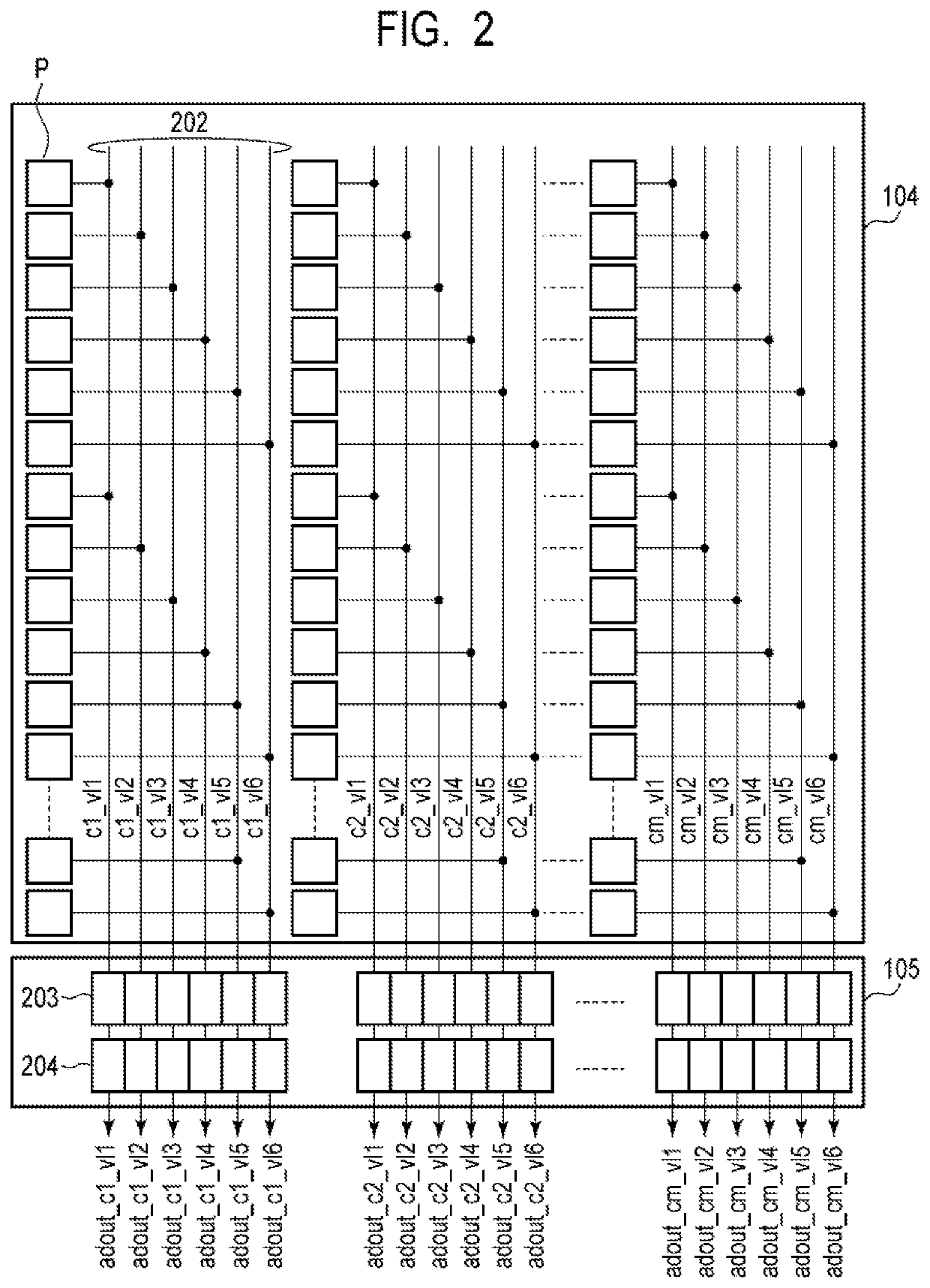
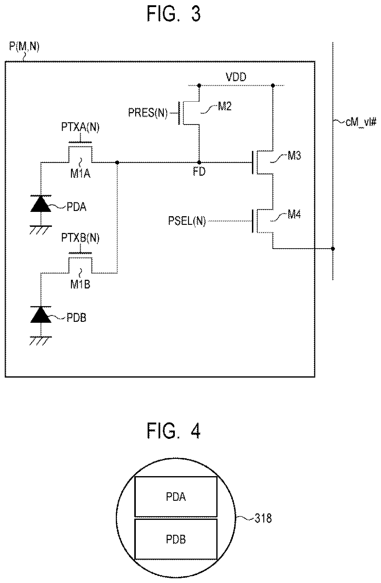
[0025]An imaging device according to a first embodiment of the present invention will be described with reference to FIG. 1 to FIG. 7. FIG. 1 is a block diagram illustrating a general configuration of the imaging device according to the present embodiment. FIG. 2 is a schematic diagram illustrating a configuration example of a pixel unit and an AD conversion unit in the imaging device according to the present embodiment. FIG. 3 is an equivalent circuit diagram illustrating a configuration example of a pixel in the imaging device according to the present embodiment. FIG. 4 is a schematic top view of a pixel in the imaging device according to the present embodiment. FIG. 5 is a schematic diagram illustrating a configuration example of a horizontal transfer unit in the imaging device according to the present embodiment. FIG. 6 is a schematic diagram illustrating a configuration example of a control unit in the imaging device according to the present embodiment. FIG. 7 is a schematic di...

second embodiment

[0103]An imaging device according to a second embodiment of the present invention will be described with reference to FIG. 11. The same components as those in the imaging device according to the first embodiment are labeled with the same references, and the description thereof will be omitted or simplified. FIG. 11 is a schematic diagram illustrating a configuration example of a data processing unit in the imaging device according to the present embodiment.

[0104]The overall configuration of the imaging device according to the present embodiment is the same as the imaging device according to the first embodiment illustrated in FIG. 1. The configuration of the imaging device according to the present embodiment will be described below mainly for features different from the imaging device according to the first embodiment.

[0105]Although the control unit 102 in the imaging device of the present embodiment is the same as the control unit 102 in the imaging device of the first embodiment i...

third embodiment

[0164]A method of driving an imaging device according to a third embodiment of the present invention will be described with reference to FIG. 9A and FIG. 9B. The same components as those in the imaging device according to the first and second embodiments are labeled with the same references, and the description thereof will be omitted or simplified.

[0165]The first embodiment is configured such that some of focus detection data stored in the data processing unit 107 are not output, and thereby one horizontal period is shortened to increase the readout rate. In such a case, focus detection data that are not output from the data processing unit 107 are written to the focus detection data storage unit 602 of the data processing unit 107 via AD conversion or horizontal transfer in the same manner as other data output from the data processing unit 107.

[0166]However, data which are not output from the data processing unit 107 are originally not required to be stored in the data processing ...


PUM


Abstract

An imaging device includes pixels, output lines on each column, an AD conversion unit including column AD conversion circuits connected to the output lines, a first storage unit including holding units connected to the column AD conversion circuits, a transfer unit that transfers signals in the first storage unit, a second storage unit that holds signals from the transfer unit, and an output unit that outputs signals in the second storage unit. The pixels output a first analog signal based on signal from the first photoelectric converter and a second analog signal based on signal from the first and second photoelectric converter. The AD conversion unit converts the first and second analog signals into first and second digital signals. The number of signals corresponding to the first digital signals of signals output by the output unit is less than the number of signals output in parallel from the output lines.

Description

BACKGROUND OF THE INVENTIONField of the Invention[0001]The present invention relates to an imaging device and an imaging system.Description of the Related Art[0002]In imaging devices having a function of acquiring signals for image generation and signals for focus detection, there is a demand for faster image capturing. Japanese Patent Application Laid-open No. 2013-211833 proposes a scheme to achieve faster image capturing by selecting regions that output signals for focus detection to reduce the total number of acquired signals. Japanese Patent Application Laid-open No. 2019-047267 proposes a scheme to achieve both image quality and faster image capturing by switching whether or not to output signals used for focus detection accumulated in a memory in a unit of analog-to-digital (AD) conversion so as not to affect an accumulation time period or control of an analog circuit.[0003]In general, a higher density of data acquisition regions used for focus detection improves AF performan...

Claims


Application Information

Patent Timeline
Patent Type & Authority Patents(United States)
IPC IPC(8): H04N5/232H04N5/335H04N5/353H04N5/3745H04N5/378H04N25/00
CPCH04N5/353H04N5/378H04N5/37452H04N5/37455H04N25/44H04N25/42H04N25/46H04N25/767H04N25/778H04N25/772H04N25/78H04N25/53H04N25/75H04N25/771
Inventor SHIGIYA, YOSHIKOSHIKINA, NORIYUKITAKENAKA, SHINTARO
Owner CANON KK
Features
  • R&D
  • Intellectual Property
  • Life Sciences
  • Materials
  • Tech Scout
  • Unparalleled Data Quality
  • Higher Quality Content
  • 60% Fewer Hallucinations
Learn More