Gate drive circuit, drive device, semiconductor device, and gate drive method

a technology of gate drive and drive device, which is applied in the direction of pulse technique, electronic switching, semiconductor devices, etc., can solve the problem of increasing losses, and achieve the effect of suppressing losses

Active Publication Date: 2022-03-08
FUJI ELECTRIC CO LTD
View PDF5 Cites 0 Cited by
  • Summary
  • Abstract
  • Description
  • Claims
  • Application Information

AI Technical Summary

Benefits of technology

[0013]Also, the present disclosure provides a gate drive method for driving a gate of a main circuit element including a majority carrier device by a drive unit, the gate drive method including: causing the drive unit to increase a drive capability of turning on the main circuit element as a main circuit current that flows through the main circuit element decreases.
[0014]According to the present disclosure, it is possible to provide a gate drive circuit, a drive device, a semiconductor device, and a gate drive method capable of suppressing losses that occur in a main circuit element including a majority carrier device.

Problems solved by technology

However, in a case of driving a gate of a main circuit element including a majority carrier device in which majority carriers contribute to electrical conduction, in a conventional manner, losses may be increased.

Method used


Image

  • Gate drive circuit, drive device, semiconductor device, and gate drive method
  • Gate drive circuit, drive device, semiconductor device, and gate drive method
  • Gate drive circuit, drive device, semiconductor device, and gate drive method

Examples


Embodiment Construction

[0028]In the following, an embodiment according to the present disclosure will be described with reference to the drawings.

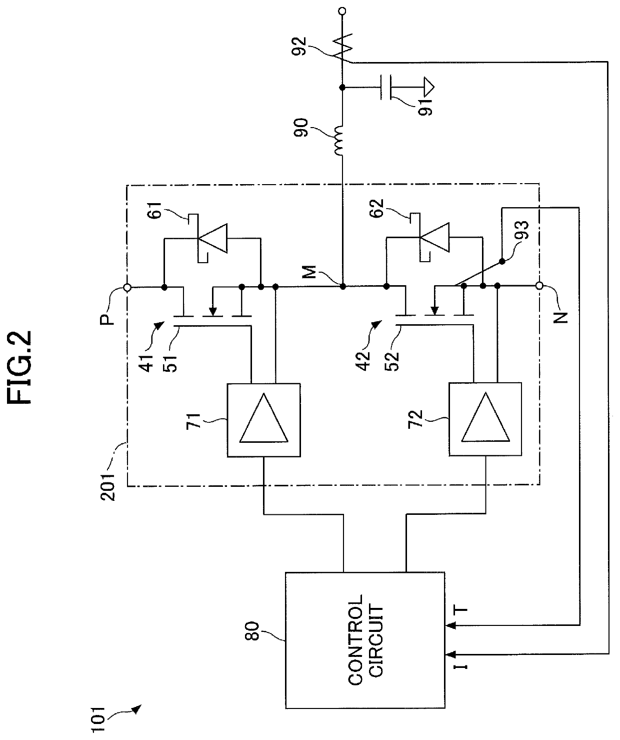
[0029]FIG. 2 is a diagram illustrating a configuration example of a semiconductor device 101 including a gate drive circuit according to an embodiment. The semiconductor device 101 illustrated in FIG. 2 is a power converter that uses a high-side switching element 51 and a low-side switching element 52 to convert DC input power to desired DC or AC output power. A load (not illustrated) is connected to a connection point M between the switching element 51 and the switching element 52 and, in the case of FIG. 2, the load (not illustrated) is connected via a coil 90. One end of the coil 90 is connected to the connection point M, and one end of a capacitor 91 is connected to the other end of the coil 90. The other end of the capacitor 91 is electrically connectable to a low power supply potential portion N.

[0030]The semiconductor device 101 includes a drive device 20...


PUM


Abstract

A gate drive circuit includes: a drive unit configured to drive a gate of a main circuit element including a majority carrier device; and a drive capability change unit configured to cause the drive unit to increase a drive capability of turning on the main circuit element as a main circuit current that flows through the main circuit element decreases.

Description

CROSS-REFERENCE TO RELATED APPLICATION[0001]This application is based upon and claims priority to Japanese Patent Application No. 2019-152222, filed on Aug. 22, 2019, the entire contents of which are incorporated herein by reference.BACKGROUND OF THE INVENTION1. Field of the Invention[0002]The present invention relates to a gate drive circuit, a drive device, a semiconductor device, and a gate drive method.2. Description of the Related Art[0003]FIG. 1 is a circuit diagram illustrating a switching power supply device 100 including a gate drive circuit 10. The gate drive circuit 10 illustrated in FIG. 1 includes gate resistors connected to a main switching element 20, and the gate resistors include voltage controlled resistors 11-1 and 11-2 of which the resistance value can be continuously changed. Further, the gate drive circuit 10 includes switching elements 14-1 and 14-2 and a signal source 15. Further, a freewheeling diode 30 is connected to the main switching element 20 in antipa...

Claims


Application Information

Patent Timeline
Patent Type & Authority Patents(United States)
IPC IPC(8): H03K3/012H03K17/687
CPCH03K3/012H03K17/687H03K17/04206
Inventor LU, HONG-FEI
Owner FUJI ELECTRIC CO LTD
Why Eureka
Try Eureka