Supercharge Your Innovation With Domain-Expert AI Agents!

Printed circuit board and motherboard with the same

a printed circuit board and mother board technology, applied in the direction of cross-talk/noise/interference reduction, electrical apparatus contruction details, printed circuit non-printed electric components association, etc., can solve the problem that anti-electromagnetic interference technologies are not applicable to open-type circuit board products such as motherboards, graphics cards,

Active Publication Date: 2022-03-22
ASUSTEK COMPUTER INC
View PDF18 Cites 0 Cited by
  • Summary
  • Abstract
  • Description
  • Claims
  • Application Information

AI Technical Summary

Benefits of technology

The patent describes a printed circuit board and a motherboard with an anti-electromagnetic interference coating. The coating includes wave-absorption powders and an adhesive material, which helps to reduce interference between the circuit board and other electronic components. The specific embodiments of the invention are further described in the accompanying drawings. The technical effect of this patent is to improve the performance and reliability of electronic devices that use printed circuit boards.

Problems solved by technology

However, such anti-electromagnetic interference technologies are not applicable to open type circuit board products such as motherboards, graphics cards, and the like.

Method used


Image

  • Printed circuit board and motherboard with the same
  • Printed circuit board and motherboard with the same
  • Printed circuit board and motherboard with the same

Examples


Embodiment Construction

[0013]Specific embodiments of the disclosure are further described in detail below with reference to schematic diagrams. Features and advantages of the disclosure are more clear based on the following descriptions and claims. Accompanying drawings which are in simplified forms and are not drawn to scale are merely used for facilitating a clear understanding of the embodiments of the disclosure.

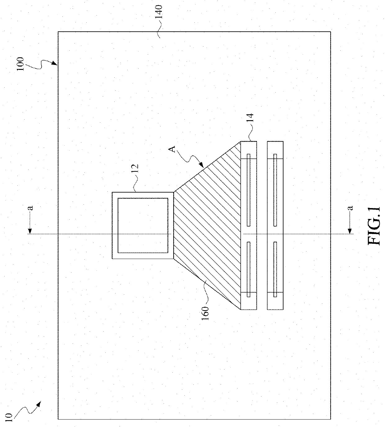
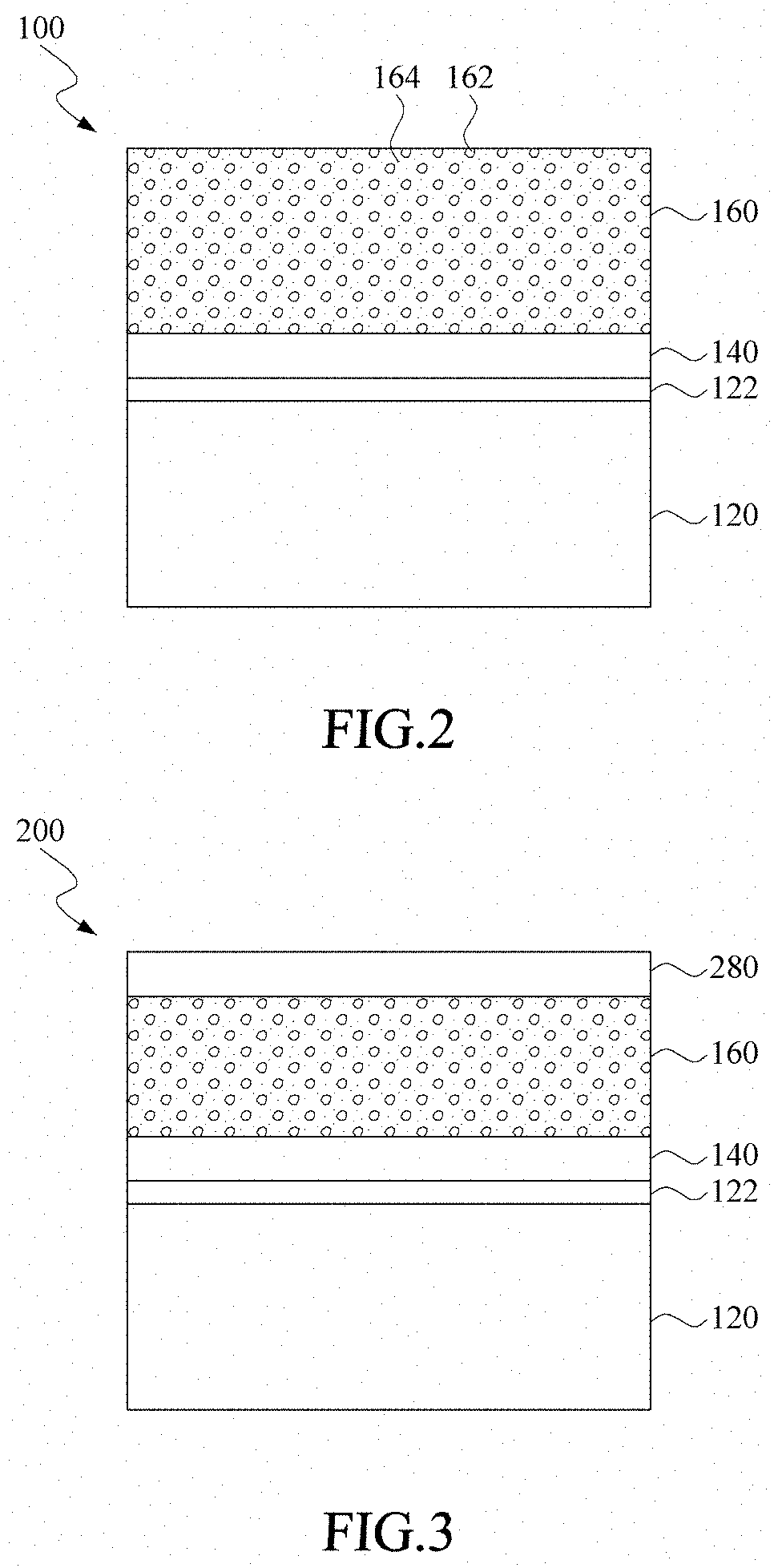
[0014]FIG. 1 is a three-dimensional schematic diagram of an embodiment of a motherboard according to the disclosure. FIG. 2 is a cross-sectional schematic diagram of an embodiment of a printed circuit board according to the disclosure, and the cross-sectional schematic diagram corresponds to an a-a cross-section in FIG. 1.

[0015]As shown in the figure, a motherboard 10 includes a printed circuit board 100, a central processing unit slot 12, and at least a memory slot 14. In an embodiment, two memory slots are taken and shows in the figure as an example.

[0016]As shown in FIG. 2, the printed circ...


PUM


Abstract

A printed circuit board comprising a main body, a first insulation layer, and an anti-electromagnetic interference (EMI) coating is provided. The first insulation layer covers the main body and comprises a predetermined area. The anti-EMI coating covers the predetermined area, and comprises wave-absorption powders and an adhesive material. A motherboard with the printed circuit board is also provided.

Description

CROSS-REFERENCE TO RELATED APPLICATION[0001]This application claims the priority benefit of Taiwan Application Serial No. 108118150, filed on May 24, 2019. The entirety of the above-mentioned patent application is hereby incorporated by reference herein and made a part of specification.BACKGROUND OF THE INVENTIONField of the Invention[0002]The disclosure relates to a printed circuit board and a mother board with the printed circuit board, and in particular to, an anti-electromagnetic interference printed circuit board and a motherboard with the printed circuit board.Description of the Related Art[0003]The conventional anti-electromagnetic interference technologies are mainly for shielding electromagnetic signal sources, for example, integrated circuit chips and integrated circuit packages, to protect electronic components in electronic products. However, such anti-electromagnetic interference technologies are not applicable to open type circuit board products such as motherboards, g...

Claims


Application Information

Patent Timeline
Patent Type & Authority Patents(United States)
IPC IPC(8): H05K7/00H05K1/02H05K1/18
CPCH05K1/0218H05K1/181H05K2201/0715H05K2201/10159H05K2201/10189H05K2201/10272H05K2201/0723H05K3/3452H05K2201/0215H05K2201/0323H05K2201/0195
Inventor TSOU, PING-HANWAN, LI-CHIEN
Owner ASUSTEK COMPUTER INC
Features
  • R&D
  • Intellectual Property
  • Life Sciences
  • Materials
  • Tech Scout
  • Unparalleled Data Quality
  • Higher Quality Content
  • 60% Fewer Hallucinations
Learn More