
Touch display device

a display device and touch technology, applied in static indicating devices, solid-state devices, instruments, etc., can solve the problems of parasitic capacitance increase or larger bezels, and achieve the effect of reducing bezel size, preventing parasitic capacitance caused by touch routing lines, and improving touch sensitivity

Active Publication Date: 2022-04-26
LG DISPLAY CO LTD
View PDF6 Cites 1 Cited by
  • Summary
  • Abstract
  • Description
  • Claims
  • Application Information

AI Technical Summary

Benefits of technology

[0035]According to the embodiments of the present disclosure, a bezel size can be reduced through the multilayer structure of touch routing lines connecting a touch sensor to a touch sensing circuit even when the touch routing lines are disposed in a non-display area.
[0036]According to the embodiments of the present disclosure, parasitic capacitance which can be caused by the touch routing lines can be prevented from being formed by changing the arrangement structure of touch routing lines connecting a touch sensor to a touch sensing circuit in consideration of the location of a common electrode, so that touch sensitivity can be improved.
[0037]According to the embodiments of the present disclosure, it is possible to provide a touch display device having an improved arrangement structure of touch routing lines suitable for a double routing structure.
[0038]According to the embodiments of the present disclosure, it is possible to provide a touch display device having an improved arrangement structure of touch routing lines suitable for a single routing structure.
[0039]According to the embodiments of the present disclosure, it is possible to provide a touch display device having an improved arrangement structure of touch routing lines suitable for a half-single routing structure.

Problems solved by technology

In the case of such display panels, due to the embedded touch sensor, there may arise a limitation in that a bezel becomes larger or parasitic capacitance is increased.

Method used


Image

  • Touch display device
  • Touch display device
  • Touch display device

Examples


Embodiment Construction

[0060]In the following description of examples or embodiments of the present disclosure, reference will be made to the accompanying drawings in which it is shown by way of illustration specific examples or embodiments that can be implemented, and in which the same reference numerals and symbols can be used to designate the same or like components even when they are shown in different accompanying drawings from one another. Further, in the following description of examples or embodiments of the present disclosure, detailed descriptions of well-known functions and components incorporated herein will be omitted when it is determined that the description can make the subject matter in some embodiments of the present disclosure rather unclear. The terms such as “including”, “having”, “containing”, “constituting”“made up of”, and “formed of” used herein are generally intended to allow other components to be added unless the terms are used with the term “only”. As used herein, singular for...


PUM


Abstract

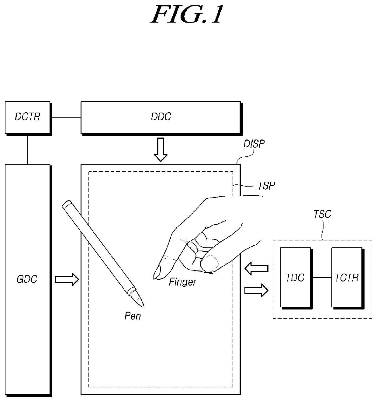
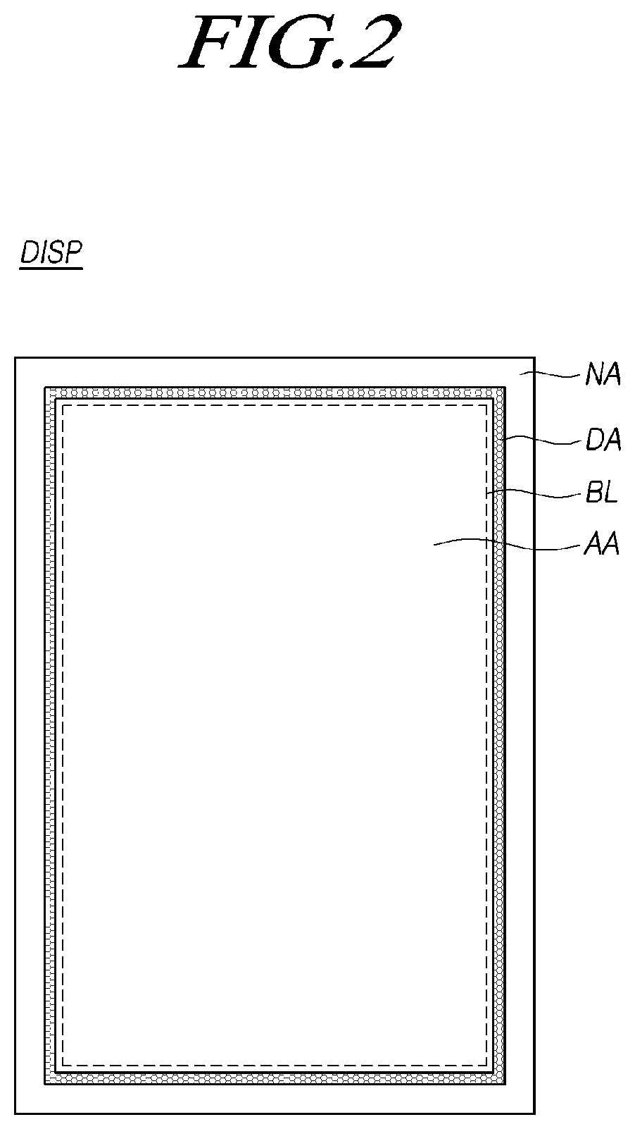
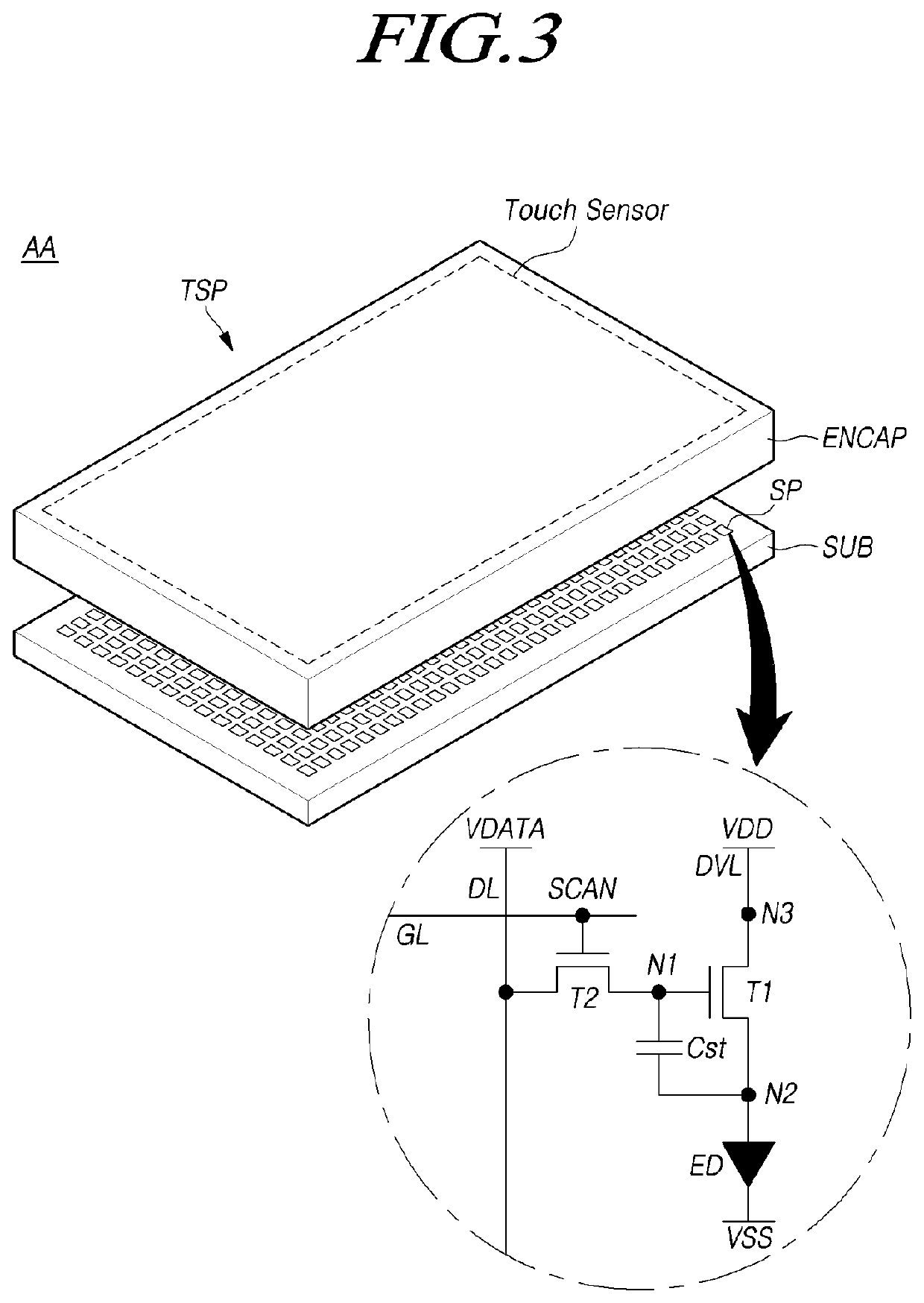
Embodiments of the present disclosure relate to a touch display device, and more particularly, to a touch display device which can have a small bezel size even when touch routing lines connecting a touch sensor to a touch sensing circuit are disposed in a non-display area and which can improve touch sensitivity by preventing or minimizing the formation of parasitic capacitance that can be caused by the touch routing lines.

Description

CROSS REFERENCE TO RELATED APPLICATION[0001]This application claims priority to Korean Patent Application No. 10-2019-0088386, filed on Jul. 22, 2019 in the Republic of Korea, the entire contents of which are hereby incorporated by reference for all purposes as if fully set forth herein into the present application.BACKGROUND OF THE INVENTION1. Field of the Invention[0002]Embodiments of the present disclosure relate to a touch display device.2. Discussion of Related Art[0003]Touch display devices are devices capable of providing a touch-based input function that allows a user to easily input information or commands intuitively and conveniently, in addition to a display function of displaying a video or an image.[0004]In order to provide the touch-based input function, such touch display devices need to identify the presence or absence of a user's touch and accurately sense touch coordinates. To this end, the touch display device includes a touch sensor, a touch sensing circuit, touc...

Claims


Application Information

Patent Timeline
Patent Type & Authority Patents(United States)
IPC IPC(8): G06F3/041G06F3/044H01L27/32H01L51/52G09G3/3266
CPCG06F3/0412G06F3/0445G06F3/0446G06F3/04164H01L27/323H01L27/3276H01L51/5253G06F2203/04111G06F2203/04112G09G3/3266G06F3/047G06F3/044H10K59/873G09G3/3225G09G3/3233G09G2300/0426G09G2300/0819G09G2300/0842G09G2300/0861G09G2310/0281G09G2300/023G09G2354/00H10K59/40H10K59/131G06F3/0416G06F2203/04103H10K50/844
Inventor LEE, HWIDEUKLEE, YANGSIK
Owner LG DISPLAY CO LTD
Learn More