Array substrate and display panel

a display panel and substrate technology, applied in the field of display panels, can solve the problems of affecting the coexistence of photography and display, affecting the image quality of the display panel, and the risk of disruption of the imaging of the camera which requires high display accuracy, so as to reduce the interference and diffraction of light, increase the refraction angle, and increase the light transmittance of the display panel

Active Publication Date: 2022-04-26
WUHAN CHINA STAR OPTOELECTRONICS SEMICON DISPLAY TECH CO LTD
View PDF10 Cites 0 Cited by
  • Summary
  • Abstract
  • Description
  • Claims
  • Application Information

AI Technical Summary

Benefits of technology

[0005]In order to solve the above problem, embodiments of the present disclosure provide an array substrate and a display panel, which can effectively solve a problem of interference and diffraction of light.
[0010]Further, a through hole is provided at a layer being the lowest within the non-wiring layer, and the through hole is configured to enhance light transmittance of the non-wiring layer.
[0015]Advantages of the present disclosure are that, by providing a combined structure (such as the first film layer and the second film layer), the light producing interference and diffraction is emitted from an optically dense medium region (such as the first film layer) to an optically sparse medium region (such as the second film layer), resulting in that the light with a larger incident angle is totally reflected. In addition, even if the light with a smaller incident angle cannot be totally reflected, when the light with the smaller incident angle passes through this combined structure, a refraction angle will be increased. Thus, it can reduce the light producing interference and diffraction to enter a camera, to make the imaging of the camera below the screen free from the light producing interference and diffraction. In addition, by providing the through hole, light transmittance of the display panel is increased to make the camera shoot better.

Problems solved by technology

In order to realize a higher screen occupation ratio, a camera under a screen is a feasible and effective solution, but how to achieve a coexistence of photography and display is a technical problem.
Visible light is extremely prone to interference and diffraction after passing through the display panel.
There is a great risk of disruption for imaging by a camera which requires high display accuracy.
Therefore, how to avoid interference and diffraction of transmitting light, resulting in the disruption to the imaging by the camera, is an important issue that needs to be solved urgently.

Method used


Image

  • Array substrate and display panel
  • Array substrate and display panel
  • Array substrate and display panel

Examples


first embodiment

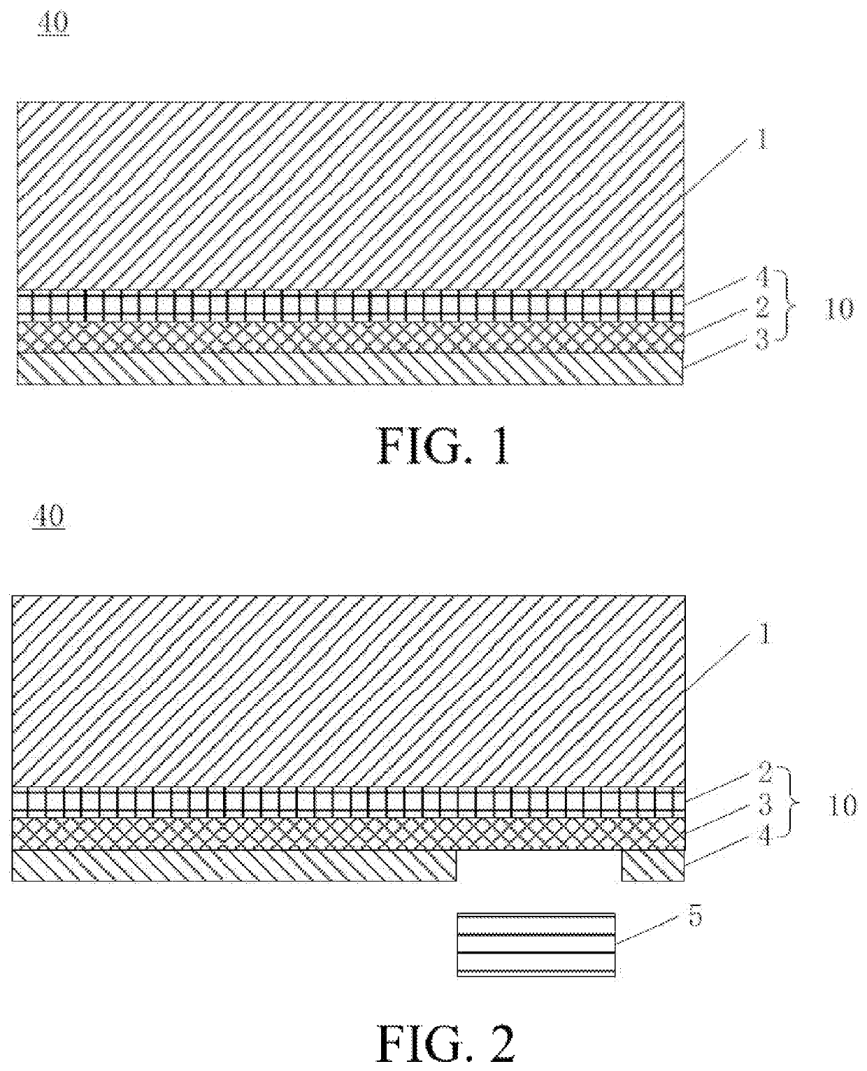
[0025]As shown in FIG. 1, which is a schematic structural diagram illustrating an array substrate provided by the present disclosure, in which the array substrate includes a wiring layer 1 and a non-wiring layer 10.

[0026]As shown in FIG. 4, in which the wiring layer 1 includes metal film layers (such as a gate layer 15). The metal film layers interfere and diffract light, and therefore interfere with imaging by a camera below a display panel.

[0027]The wiring layer 1 mainly includes an active layer 11, a source electrode layer 16, a drain electrode layer 17, the gate 15, a gate insulation layer 14, an interlayer dielectric layer 12, and a passivation layer 13.

[0028]The active layer 11 is disposed on the non-wiring layer 10. A material of the active layer 11 is an oxide, wherein a material of the oxide may be indium gallium zinc oxide (IGZO), indium zinc tin oxide (IZTO), indium gallium zinc tin oxide (IGZTO), and the like. A thickness of which ranges from 100 to 1000 Angstroms. In a ...

second embodiment

[0038]As shown in FIG. 2, which is a schematic structural diagram illustrating an array substrate provided by the present disclosure, in which the array substrate includes a wiring layer 1 and a non-wiring layer 10.

[0039]In the second embodiment of the present disclosure, the non-wiring 10 includes a first film layer 2, a second film layer 3, and a third film layer 4. The third film layer 4 is disposed on a bottom portion of the wiring layer 1. The first film layer 2 is disposed adjacent to the third film layer 4 and is located on a bottom portion of the third film layer 4. The second film layer 3 is disposed adjacent to the first film layer 2 and is located on a bottom portion of the first film layer 2.

[0040]As shown in FIG. 4, the wiring layer 1 includes metal film layers (such as the gate layer 15). The metal film layers interfere and diffract light, and therefore interfere with imaging by a camera below a display panel.

[0041]The wiring layer 1 mainly includes an active layer 11,...

third embodiment

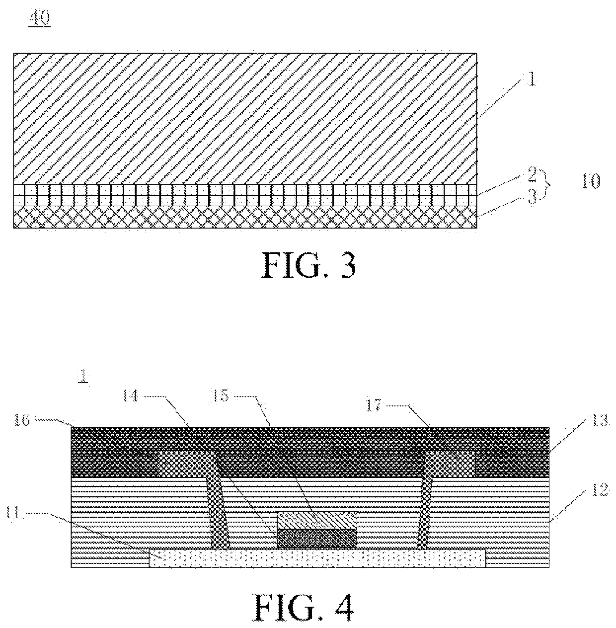
[0051]As shown in FIG. 3, which is a schematic structural diagram illustrating an array substrate provided by the present disclosure.

[0052]In the third embodiment, the non-wiring 10 only includes a first film layer 2 and a second film layer 3. The first film layer 2 is disposed on a bottom portion of the wiring layer 1. The second film layer 3 is disposed adjacent to the first film layer 2 and is located on a bottom portion of the first film layer 2. In the third embodiment, except for different features described here, the other features are the same as those of the second embodiment, and no more description here.

[0053]Advantages of the third embodiment of the present disclosure are that, by providing a combined structure (such as the first film layer and the second film layer), the light producing interference and diffraction is emitted from the optically dense medium region (such as the first film layer) to the optically sparse medium region (such as the second film layer), resul...


PUM

PropertyMeasurementUnit
refractive indexaaaaaaaaaa
thicknessaaaaaaaaaa
thicknessaaaaaaaaaa

Abstract

The present disclosure provides an array substrate and a display panel. The array substrate includes a wiring layer, and a non-wiring layer located on a bottom portion of the wiring layer. The non-wiring layer includes a first film layer and a second film layer, which are sequentially stacked in a direction away from the wiring layer. A refractive index of the second film layer is smaller than a refractive index of the first film layer.

Description

[0001]This application claims priority from a Chinese patent application filed in the Chinese Patent Office on Oct. 8, 2019, with application number 201910951289.8, and is titled as “array substrate and display panel”, the entire contents of which are incorporated herein by reference.FIELD OF THE INVENTION[0002]The present disclosure relates to the technical field of displays, and specifically to an array substrate and a display panel.BACKGROUND OF THE INVENTION[0003]Electronic devices provided with a high screen occupation ratio are increasingly favored by consumers. The screen occupation ratio refers to a relative ratio of an area of a screen to a front panel of an electronic product, which is a parameter that makes an appearance design of the electronic product easier to obtain a visual favorable impression. The screen occupation ratio of current electronic products is relatively small. In particular, upper and lower bezels occupy a large screen occupation ratio due to handset, c...

Claims


Application Information

Patent Timeline
Patent Type & Authority Patents(United States)
IPC IPC(8): H01L27/12
CPCH01L27/1248G02F1/1362G02F1/136286G02F1/1335H01L27/1225G02F1/133345G02F1/1333
Inventor ZHAO, XIAOFENG
Owner WUHAN CHINA STAR OPTOELECTRONICS SEMICON DISPLAY TECH CO LTD
Why Eureka
Try Eureka