Electron beam system for inspection and review of 3D devices

a technology of electromagnetic beams and 3d devices, applied in the direction of electrical discharge tubes, semiconductor/solid-state device testing/measurement, electrical apparatus, etc., can solve the problems of affecting the electrical parameters of the device, the operation of semiconductor manufacturing processes closer to the limitation of the performance capability of the process, and the need to detect defects of decreasing size, etc., to achieve the effect of low landing energy

Active Publication Date: 2022-05-17
KLA CORP
View PDF22 Cites 0 Cited by
  • Summary
  • Abstract
  • Description
  • Claims
  • Application Information

AI Technical Summary

Problems solved by technology

However, as the dimensions of semiconductor devices decrease, inspection becomes even more important to the successful manufacture of acceptable semiconductor devices because smaller defects can cause the devices to fail.
For instance, as the dimensions of semiconductor devices decrease, detection of defects of decreasing size has become necessary because even relatively small defects may cause unwanted aberrations in the semiconductor devices.
As design rules shrink, however, semiconductor manufacturing processes may be operating closer to the limitation on the performance capability of the processes.
In addition, smaller defects can have an impact on the electrical parameters of the device as the design rules shrink, which drives more sensitive inspections.
As design rules shrink, the population of potentially yield-relevant defects detected by inspection grows dramatically, and the population of nuisance defects detected by inspection also increases dramatically.
Therefore, more defects may be detected on the wafers, and correcting the processes to eliminate all of the defects may be difficult and expensive.
Furthermore, at smaller design rules, process-induced failures, in some cases, tend to be systematic.
That is, process-induced failures tend to fail at predetermined design patterns often repeated many times within the design.
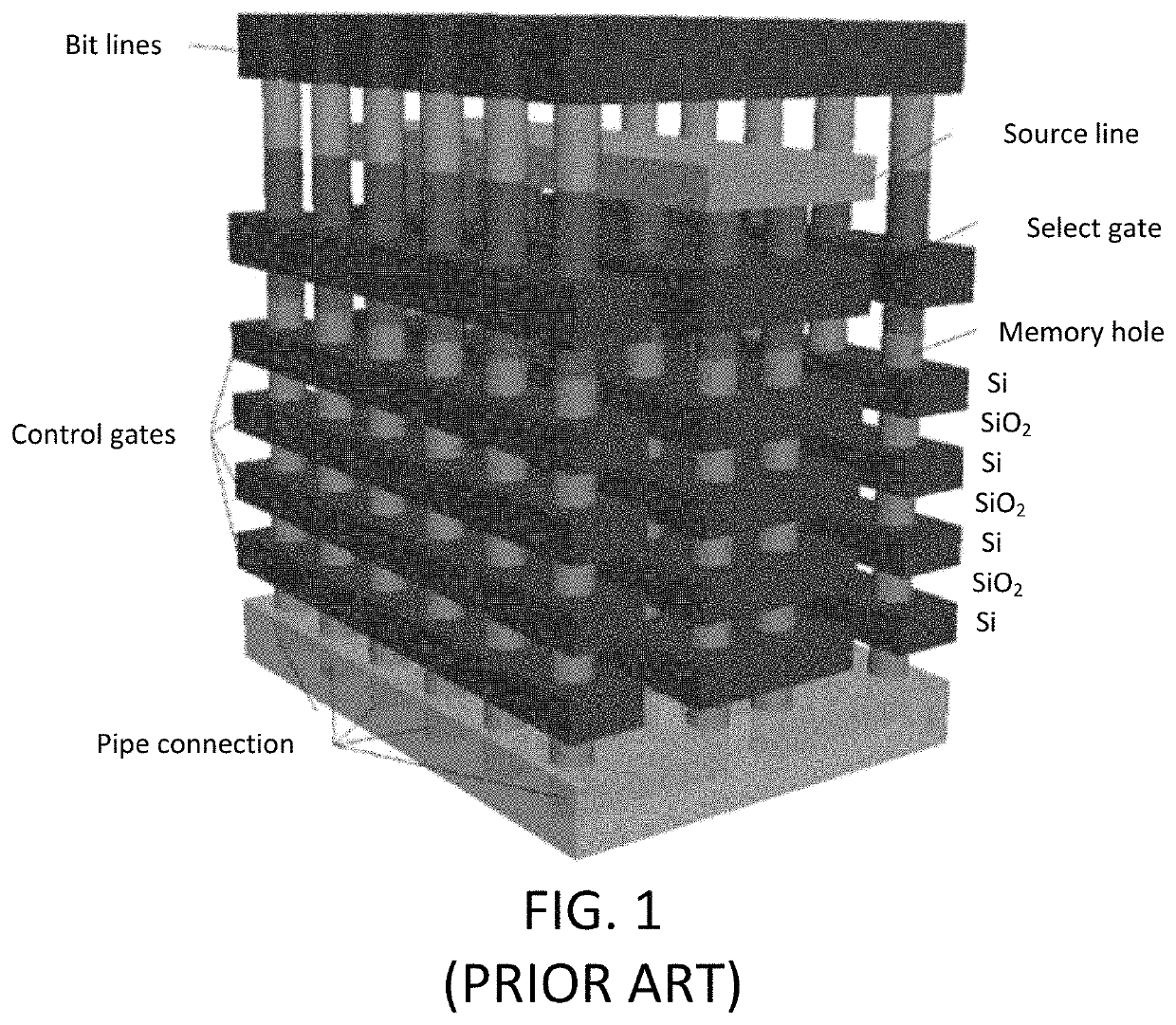
The 2D planar processes of nano-fabrications are facing bottlenecks when trying to meet the development of semiconductor chips because of physical effects that occur with the increase of the IC integration density.
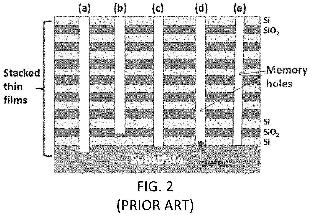
However, high uniformity etching results for hundreds of billions of memory holes with hundreds of layers of depth does not always occur due to technology limits.
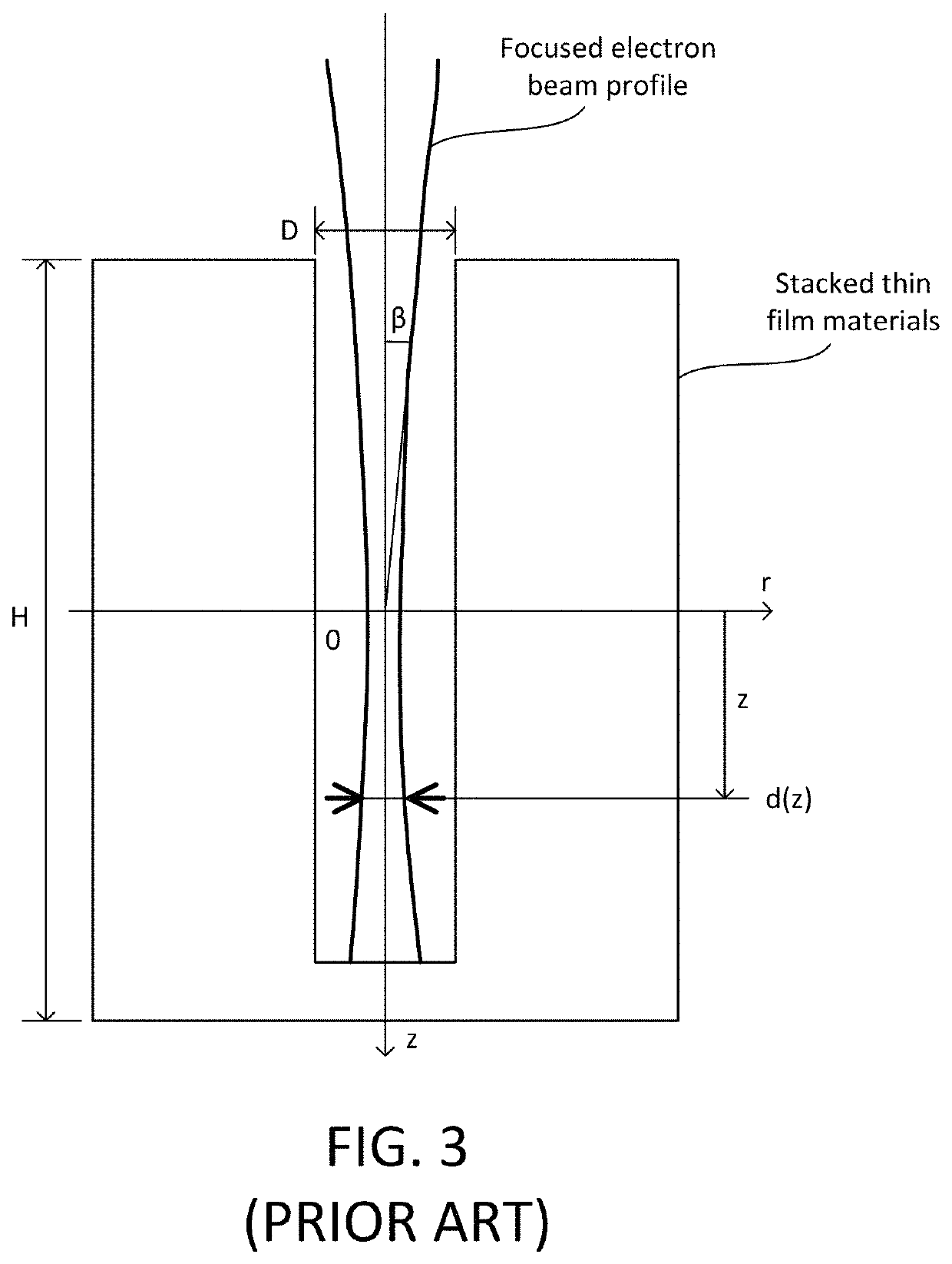
An electron beam system with tens of microns of DOF is difficult to design and implement.
However, the secondary electron signals can only reflect the characteristics from the surface of materials.
Previous electron beam systems with BSE signals used to inspect and / or review an HAR device have drawbacks.
First, these systems have limited applications.
Thus, the stacked thin film materials cannot be too thick or the BSEs will be insufficiently powered to penetrate out of the bulk of the materials.
This limits such electron beam systems to inspection and review of tens of layers of a 3D NAND flash device.
Second, previous electron beam systems with BSE signals have limited DOF of the primary electron beam.
However, the Coulomb interactions between electrons may be fairly sensitive to the beam current, causing the tails of the electron distributions to increase rapidly and further pollute the usual signal from the bottom of a memory hole.

Method used


Image

  • Electron beam system for inspection and review of 3D devices
  • Electron beam system for inspection and review of 3D devices
  • Electron beam system for inspection and review of 3D devices

Examples


first embodiment

[0062]FIG. 6(a) shows an electron beam system 100. FIG. 6(b) shows the schematic of the optics of the embodiment of FIG. 6(a). A magnetic gun lens may be used in the electron beam system 100. This can reduce the gun lens aberrations, such that the blurs at the wafer side from the gun are negligibly dominant even though the optical magnification is increased for smaller NA or larger DOF. This also can enable focus / defocus of the high voltage electron beam to select a desired beam current.

[0063]The electron beam system 100 includes an electron beam source 101 that generates an electron beam 103. The electron beam 103 is directed at a wafer 110, which can be positioned on a platen. The electron beam source 101 can include a tip with a radius less than 1 μm, such as from approximately 0.3 μm to less than 1.0 μm. The electron beam source 101 also can include an extractor 115, anode 116, gun magnetic lens coil 117, and gun magnetic lens pole pieces 118. These components can be part of the...

second embodiment

[0081]FIG. 8 is a system for BSE detection. The annular detector 109 for detecting BSEs around the optical axis may be at least partly inside the upper Wehnelt electrode 107. In an instance, a surface of the annular detector 109 can be exposed to BSEs. In another instance, the annular detector 109 is totally inside the upper Wehnelt electrode 107 without exposure to the BSEs, which still allows BSE collection.

[0082]The upper Wehnelt electrode 107 may either be floated or grounded. The lower Wehnelt electrode 108 can be used to charge the wafer for a required extracting field. With the same conditions as those for FIGS. 7(a) and 7(b), the simulations for ray-tracing the BSEs from the bottom of a 3D NAND memory hole show high collection efficiency. Thus, the BSEs with the polar angles from approximately 10 to 60 degrees may be detected. Because of the characteristics of the BSE angular distributions, most of the total emitted BSEs have been included in the angles of from approximately...

third embodiment

[0083]FIG. 9 is an electron beam splitting optics with three magnetic deflectors. In the embodiment of FIG. 9, the deflector 106 is a magnetic deflector (MD-3). For only collecting and using the high energy BSEs to inspect high AR devices like 3D NAND memories, an optical design like a conventional Wien filter for splitting the BSEs from the PEs (primary electrons) is not required.

[0084]The system also includes an upper magnetic deflector 121 (MD-1) and a middle magnetic deflector 122 (MD-2) disposed in the path of the electron beam 103 between the deflector 106 and the magnetic condenser lens 105. The upper magnetic deflector 121 is disposed in the path of the electron beam 103 between the deflector 106 and the magnetic condenser lens 105. The middle magnetic deflector 122 is disposed in the path of the electron beam 103 between the upper magnetic deflector 121 and the magnetic deflector 106.

[0085]The upper magnetic deflector 121 can be configured to deflect the electron beam 103 t...


PUM


Abstract

An electron beam system for wafer inspection and review of 3D devices provides a depth of focus up to 20 microns. To inspect and review wafer surfaces or sub-micron-below surface defects with low landing energies in hundreds to thousands of electron Volts, a Wien-filter-free beam splitting optics with three magnetic deflectors can be used with an energy-boosting upper Wehnelt electrode to reduce spherical and chromatic aberration coefficients of the objective lens.

Description

CROSS-REFERENCE TO RELATED APPLICATIONS[0001]This application claims priority to the provisional patent application filed Apr. 15, 2020 and assigned U.S. App. No. 63 / 010,097, the disclosure of which is hereby incorporated by reference.FIELD OF THE DISCLOSURE[0002]This disclosure relates to electron beam systems.BACKGROUND OF THE DISCLOSURE[0003]Evolution of the semiconductor manufacturing industry is placing greater demands on yield management and, in particular, on metrology and inspection systems. Critical dimensions continue to shrink, yet the industry needs to decrease time for achieving high-yield, high-value production. Minimizing the total time from detecting a yield problem to fixing it determines the return-on-investment for a semiconductor manufacturer.[0004]Fabricating semiconductor devices, such as logic and memory devices, typically includes processing a semiconductor wafer using a large number of fabrication processes to form various features and multiple levels of the...

Claims


Application Information

Patent Timeline
Patent Type & Authority Patents(United States)
IPC IPC(8): H01J37/00H01L21/66H01J37/063H01J37/065H01J37/244H01J37/14
CPCH01L22/12H01J37/063H01J37/065H01J37/14H01J37/244H01J2237/141H01J2237/152H01J37/145H01J2237/04926H01J2237/0268H01J2237/0048H01J2237/281H01J37/28H01J2237/24475H01J37/04
Inventor JIANG, XINRONGSEARS, CHRISTOPHER
Owner KLA CORP
Why Eureka
Try Eureka