
Testing method and test apparatus in semiconductor apparatus

a technology of semiconductor apparatus and test method, which is applied in the direction of digital storage, instruments, measurement devices, etc., can solve problems such as inability to correctly perform

Inactive Publication Date: 2001-07-26
MITSUBISHI ELECTRIC CORP
View PDF0 Cites 9 Cited by
  • Summary
  • Abstract
  • Description
  • Claims
  • Application Information

AI Technical Summary

Problems solved by technology

However, because the RAM built-in self-repair circuit 5 controls the redundant control circuit 3 according to a result of one test performed for the RAM 1 in the conventional test device, in cases where a fault not detected under ordinary conditions (for example, ordinary power supply voltage and temperature) set in one test exists in the RAM 1, there is a problem that a control of the RAM built-in self-repair circuit 5 for the redundant control circuit 3 to avoid the use of a portion relating to the faulty of the RAM 1 in specific conditions differing from the ordinary conditions cannot be correctly performed.
Therefore, there is a problem in cases where a self-test of the electronic system 100 for the RAM 1 is performed under a high temperature condition.

Method used


Image

  • Testing method and test apparatus in semiconductor apparatus
  • Testing method and test apparatus in semiconductor apparatus
  • Testing method and test apparatus in semiconductor apparatus

Examples


first embodiment

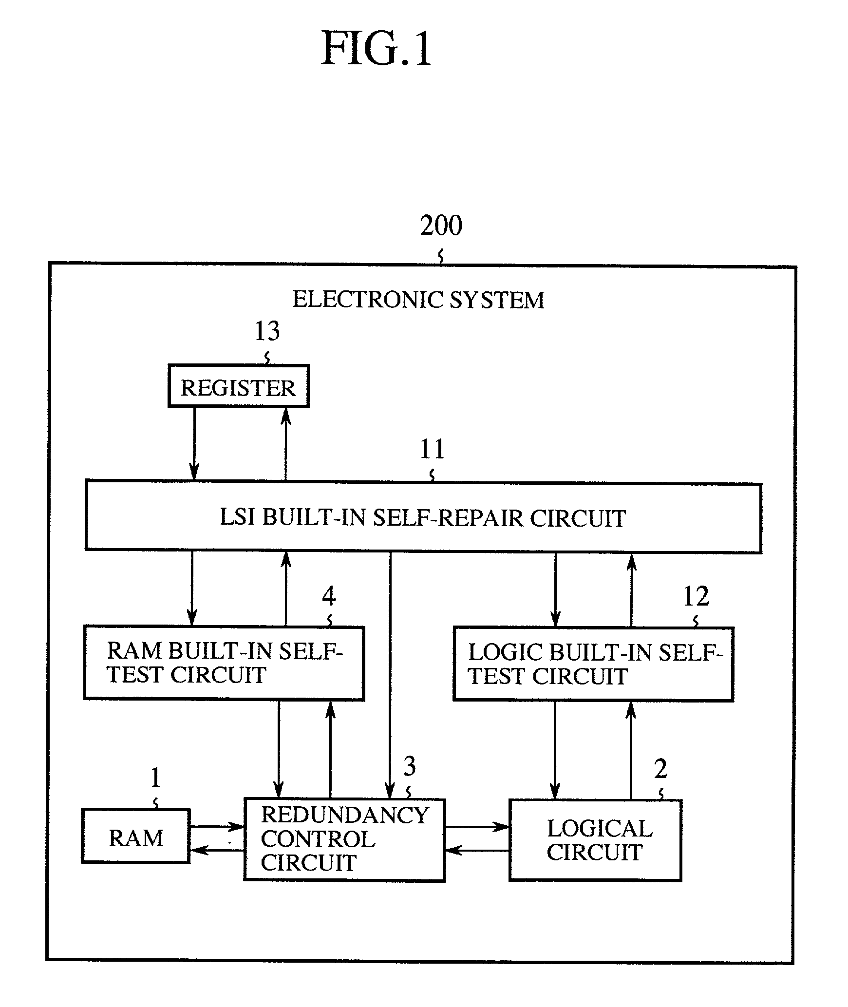
[0079] FIG. 1 is a block diagram showing the configuration of a test apparatus, which is arranged in an electronic apparatus including a to-be-tested circuit (for example, RAM) and is operated according to a testing method to test the to-be-tested circuit, according to the present invention.

[0080] In FIG. 1, a reference sign 200 indicates an electronic system operable at each of a normal operation mode and a self-repair operation mode.

[0081] A reference sign 1 indicates a RAM (functioning as a to-be-tested circuit) to be self-repaired. The RAM 1 has redundancy memory cells, so that a data storing capacity of the RAM 1 is larger than that required to perform a desired normal operation in the electronic system 200. A reference sign 2 indicates a logical circuit arranged in a periphery of the RAM 1 (functioning as a peripheral circuit). The RAM 1 and the logical circuit 2 are used in cases where the desired normal operation is performed in the electronic system 200.

[0082] A reference s...

embodiment 2

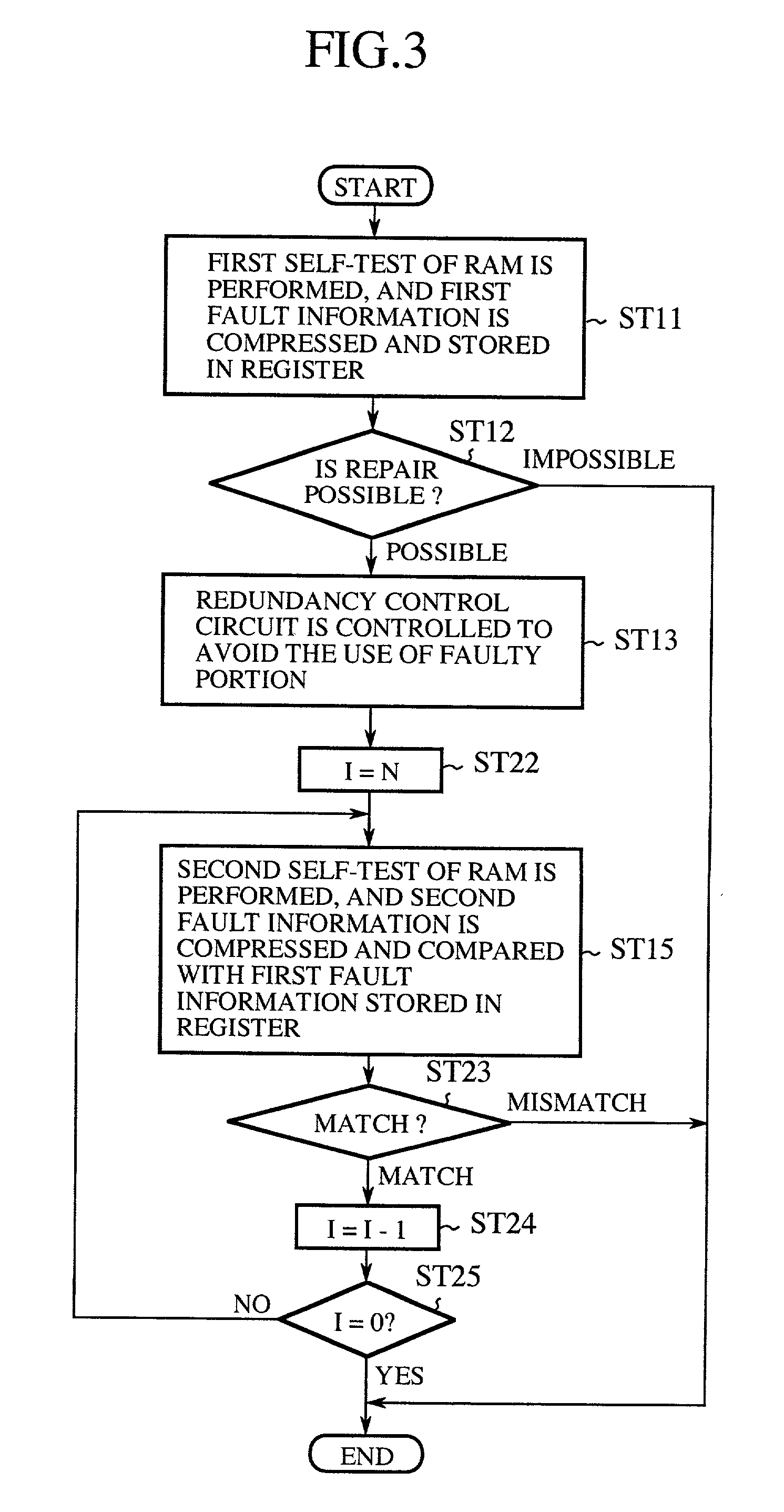
[0102] FIG. 3 is a flow chart showing a method of testing the RAM 1 in a self-repair operation according to a second embodiment of the present invention. The configuration of a test apparatus according to the second embodiment is the same as that shown in FIG. 1 of the first embodiment. Also, operations performed in the same steps as those of FIG. 2 are the same as those of the steps of FIG. 2.

second embodiment

[0103] In the testing method the first self-test (that is, the first logical test) of the RAM 1 is performed under the first test condition, and the first RAM test result (that is, the first fault information) is compressed and stored in the register 13 (the step ST11). Thereafter, the judgment whether or not the repair of the faulty portion of the RAM 1 is possible is performed (the step ST12). In cases where the repair of the faulty portion of the RAM 1 is possible, the redundant control circuit 3 is controlled to avoid the use of the faulty portion of the RAM 1 in the normal operation (the step ST13).

[0104] Thereafter, an I-th (I=2, 3, - - - , N+1) self-test of the RAM 1 is repeatedly performed N times in the same manner as the first self-test while a temperature of the semiconductor apparatus having the RAM 1 is gradually risen (steps ST22, ST24 and ST25 denoting the confirmation step), and an I-th RAM test result under an I-th test condition (or a changing test condition), in ...


PUM


Abstract

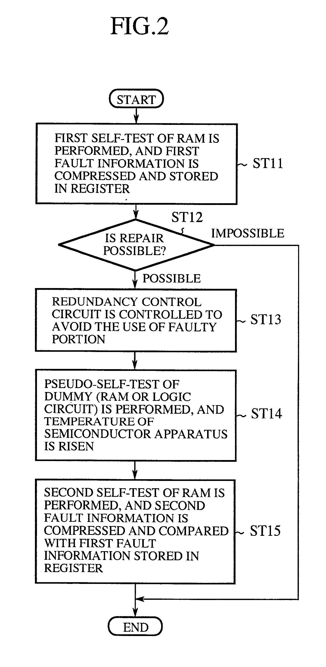
In a self-repairing operation, a first self-test of a RAM is performed at a first temperature to obtain a first RAM test result, a RAM built-in self-test circuit judges according to the first RAM test result that a faulty portion exists in the RAM, an LSI built-in self-repair circuit judges that the repair of the faulty portion of the RAM is possible, the LSI built-in self-repair circuit controls a redundancy control circuit to avoid the use of the faulty portion of the RAM in a normal operation, the temperature of the RAM is risen by operating the RAM or a logical circuit in a pseudo-self-test to change the first temperature to a second temperature, a second self-test of the RAM is performed at the second temperature to obtain a second RAM test result, and the LSI built-in self-repair circuit confirms that the repair of the faulty portion of the RAM is possible at each of the first and second temperatures by comparing the second RAM test result with the first RAM test result. Therefore, the reliability of the test of the RAM for the test condition change can be improved, and a correct operation of the RAM can be guaranteed at the first and second temperatures after a self-repair of the RAM.

Description

[0001] 1. Field of the Invention[0002] The present invention relates to a testing method and test apparatus arranged in a semiconductor apparatus in which a to-be-tested circuit such as a random access memory (RAM) arranged in the semiconductor apparatus is tested to guarantee a correctly-performed normal operation of the semiconductor apparatus on condition that a redundant circuit of the to-be-tested circuit is controlled according to a self-repair function of the semiconductor apparatus so as to avoid the use of a faulty portion of the to-be-tested circuit.[0003] 2. Description of Related Art[0004] FIG. 17 is a block diagram showing the configuration of a conventional test device arranged in an electronic system (or a semiconductor apparatus) having a self-repair function. In the conventional test device arranged in the electronic system, a random access memory (RAM) of the electronic system is self-repaired by using the conventional test device.[0005] In FIG. 17, a reference sig...

Claims


Application Information

Patent Timeline
IPC IPC(8): G11C29/00G01R31/28G11C29/50
CPCG11C29/50G11C29/72G11C29/00
Inventor MAENO, HIDESHI
Owner MITSUBISHI ELECTRIC CORP
Learn More