Phase shifting design and layout for static random access memory

a random access memory and phase shifting technology, applied in the field of phase shift masking of complex layouts, to achieve the effects of tighter packing of memory cells, improved yield, and improved integrated circuit density

Inactive Publication Date: 2002-09-12
SYNOPSYS INC
View PDF0 Cites 79 Cited by
  • Summary
  • Abstract
  • Description
  • Claims
  • Application Information

AI Technical Summary

Benefits of technology

0009] Methods and apparatuses for fully defining static random access memory (SRAM) using phase shifting layouts are described. By producing the SRAM memory using a "full phase" mask, yield can be improved at smaller sizes (relative to using the

Problems solved by technology

By placing shifters in this region, destructive interference of

Method used


Image

  • Phase shifting design and layout for static random access memory
  • Phase shifting design and layout for static random access memory
  • Phase shifting design and layout for static random access memory

Examples


Embodiment Construction

[0028] Overview

[0029] Layouts and arrangements for defining several types of patterns using phase shifting will be considered.
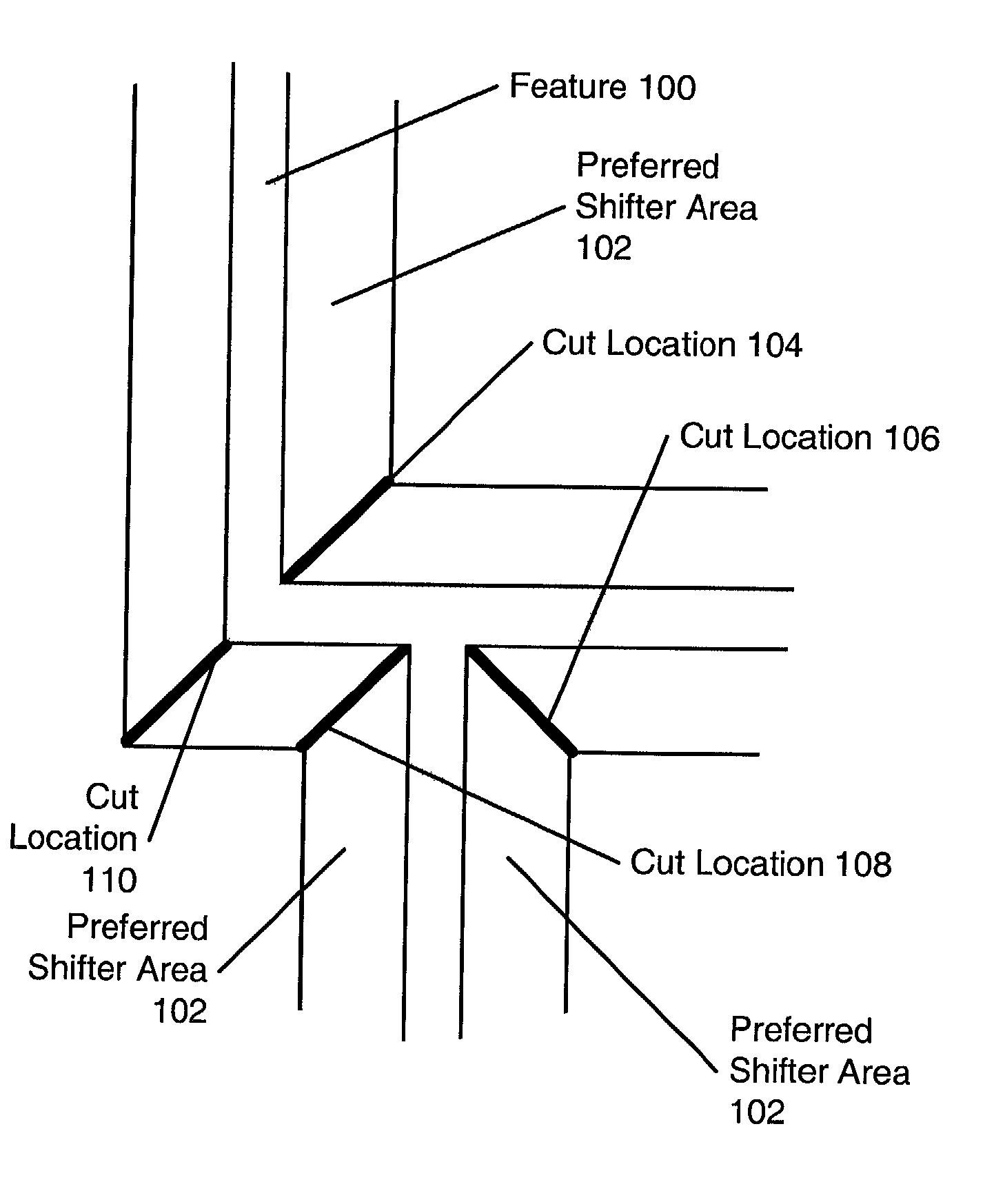
[0030] T-L Junction

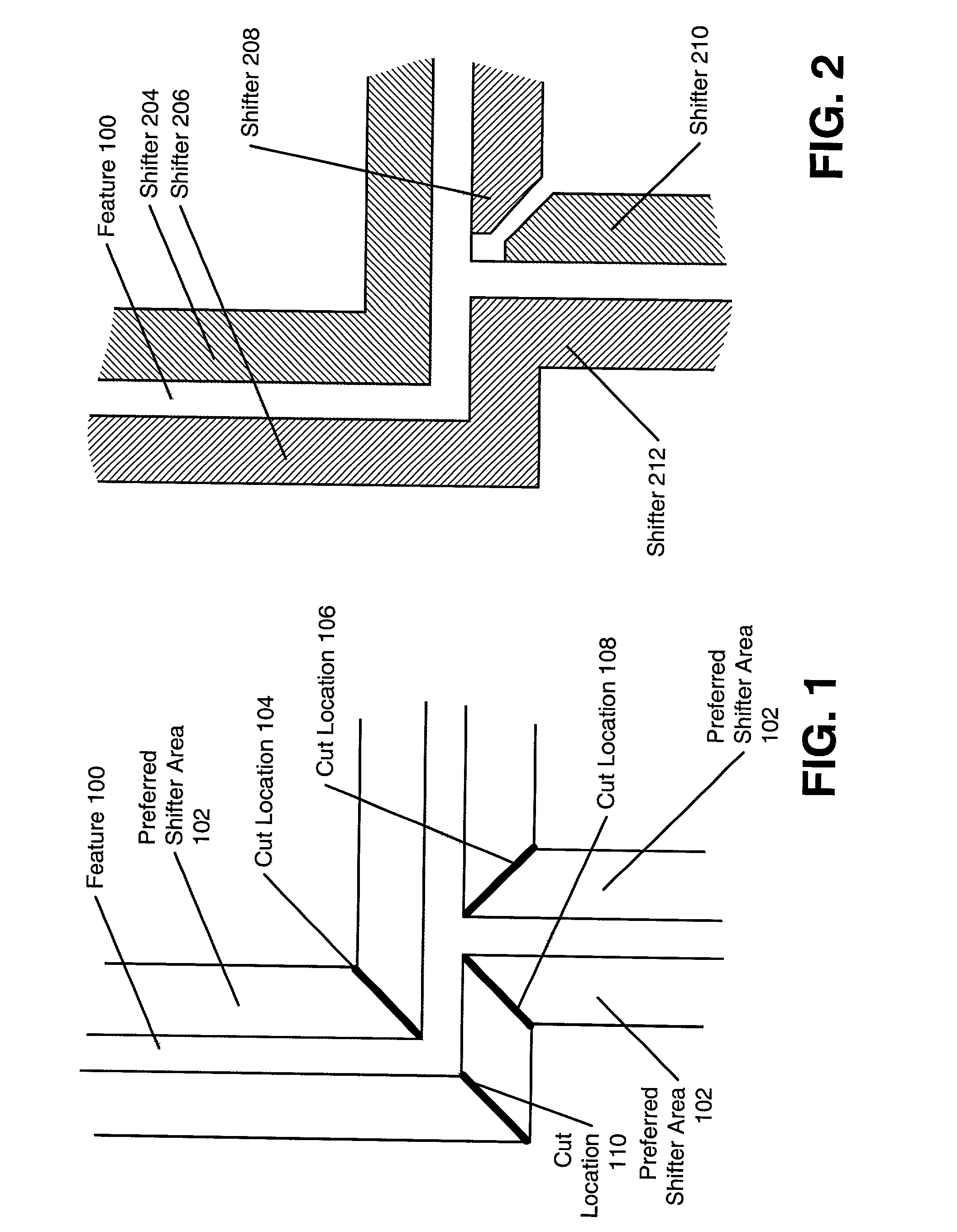
[0031] FIG. 1 illustrates a combination T-L junction, specifically the layout of FIG. 1 includes the feature 100 that includes an L shape adjacent to a T shape. A preferred shifter area 102 is shown surrounding the feature 100. The preferred shifter area 102 corresponds to the preferred phase shifter width for use in defining the feature 100 using phase shifting. Further, cutting locations where shifters defined in the preferred shifter area 102 may be placed. Specifically, the cut locations 104, 106, 108, and 110 are identified.

[0032] FIG. 2 illustrates a phase shifting layout for the T-L junction of FIG. 1. More specifically, the cut location 106 was selected--to minimize the number of cuts--and thus four shifters: the shifter 204, the shifter 206, the shifter 208, and the shifter 210, are used to define the feature 100. The phase shiftin...


PUM


Abstract

Methods and apparatuses for fully defining static random access memory (SRAM) using phase shifting layouts are described. The approach includes identifying that a layout includes SRAM cells and defining phase shifting regions in a mask description to fully define the SRAM cells. The phase conflicts between adjacent phase shifters are resolved by selecting cutting patterns designed for the SRAM shape and functional structure. Additionally, the transistor gates of the SRAM cells can be reduced in size relative to the original SRAM layout design. Thus, an SRAM cell can be lithographically printed with small, consistent critical dimensions including extremely small gate lengths resulting in higher yields and improved performance.

Description

BACKGROUND OF THE INVENTION[0001] 1. Field of the Invention[0002] The present invention relates to manufacturing small dimension features of objects, such as integrated circuits, using photolithographic masks. More particularly, the present invention relates to phase shift masking of complex layouts for integrated circuits and similar objects.[0003] 2. Description of Related Art[0004] Phase shift masking has been applied to create small dimension features in integrated circuits. Typically the features have been limited to selected elements of the design, which have a small, critical dimension. See, for example, U.S. Pat. No. 5,766,806.[0005] Although manufacturing of small dimension features in integrated circuits has resulted in improved speed and performance, it is desirable to apply phase shift masking more extensively in the manufacturing of such devices. However, the extension of phase shift masking to more complex designs results in a large increase in the complexity of the ma...

Claims


Application Information

Patent Timeline
IPC IPC(8): G03F1/00G03F1/14G03F7/20
CPCG03F1/26G03F1/30G03F1/36G03F7/70425G03F7/70433G03F7/70466G03F1/70
Inventor PIERRAT, CHRISTOPHECOTE, MICHEL LUC
Owner SYNOPSYS INC
Why Eureka
Try Eureka