Stress-relieving heatsink structure and method of attachment to an electronic package

a heatsink and stress-relief technology, applied in the direction of electrical equipment, semiconductor devices, semiconductor/solid-state device details, etc., can solve the problems of failure to provide a multi-segment heatsink arrangement and failure to provid

Inactive Publication Date: 2002-09-26
GLOBALFOUNDRIES INC
View PDF0 Cites 8 Cited by
  • Summary
  • Abstract
  • Description
  • Claims
  • Application Information

AI Technical Summary

Benefits of technology

[0019] Another object of the present invention is to provide a heatsink structure constituted of a plurality of combined smaller-sized heatsink devices or substructures which are joined along slitted edges through the intermediary of a low-stress adhesive or suitable engaging means, which will enable a certain degree of flexibility to be imparted to the overall heatsink structures so as to prevent delamination caused by heat-induced strains and stresses encountered during operation of the electronic component on which the heatsink is mounted, by a resultant reduction of the strains due to an enhanced flexibility and bendability of the heatsink structure.
[0020] Still another object of the present invention is to provide a method of forming the novel heatsink structure which is constituted of a plurality of joined or adhesively interconnected smaller heatsink components or substructures in a stress-relieving manner while the thermal conductivity of the electronic package is essentially maintained.

Problems solved by technology

The structure disclosed in this patent fails to provide a multi-segmented heatsink arrangement which is adapted to reduce thermal mechanical stresses of the heatsink when coupled to the electronic package component.
However, as in the previously discussed prior art publications, there is no low-stress interconnection between various discrete heatsink segments which are combined to form an overall heatsink arrangement which would prevent delamination of the components of the electronic package caused by heat generated by the package.
However, the stress-relief interconnections are merely constituted by reducing the thickness of part of the heatsink element to provide some bending ability, and does not in actuality produce a separate components which are adapted to be combined with other separate components to form a complete structure.
U.S. Pat. No. 4,296,455 also discloses a plurality of discrete heatsink components which do not, in actuality enable the reduction of stresses tending to delaminate the heatsink structure from the remaining portions of the electronic package to which they are fastened through the intermediary of an adhesive material, but which does not provide a unitarily connected entity.

Method used


Image

  • Stress-relieving heatsink structure and method of attachment to an electronic package
  • Stress-relieving heatsink structure and method of attachment to an electronic package
  • Stress-relieving heatsink structure and method of attachment to an electronic package

Examples


Embodiment Construction

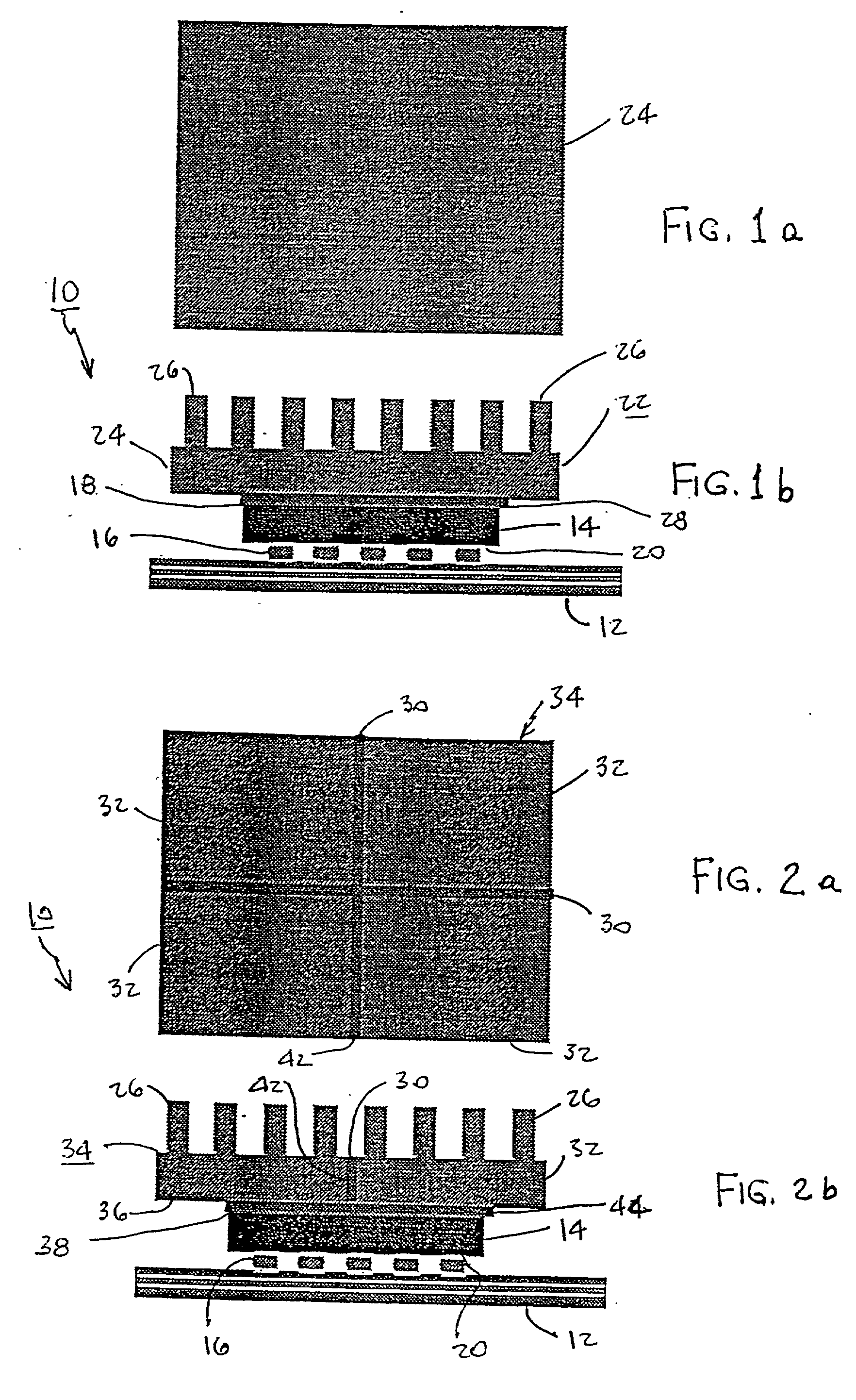
[0025] Referring now in specific detail to the drawings, and particularly FIGS. 1a and 1b, there is illustrated an electronic package which includes a heatsink in accordance with the prior art.

[0026] In particular, the electronic package 10 includes a printed or wired circuit board or card 12 which has a semiconductor chip package 14 positioned thereon, with the interposition of solder balls 16 and underfill material (not shown), as is well known in the technology.

[0027] Arranged above the semiconductor chip package 14, and facing the surface 18 thereof opposite the side 20 facing the circuit board or card 12, there is provided a heatsink structure 22 for dissipating heat generated by the electronic package 10 during operation thereof.

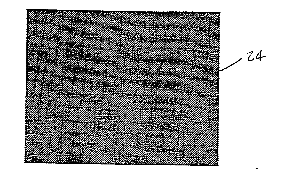
[0028] The heatsink structure 22, in this instance, is constituted of a relatively thick unitary base member 24 of generally flat or planar configuration, preferably constituted of a copper or aluminum material or composition, which extends in spaced r...


PUM


Abstract

A stress-relieving heatsink structure and method of forming thereof for an electronic package, for instance, that including a semiconductor chip package which is mounted on a wired carrier, such as a circuitized substrate. The heatsink structure is constituted from a plurality of base structures which are joined along slits so as to impart a degree of flexibility to the electronic package inhibiting the forming of stresses tending to cause delamination of the package components.

Description

[0001] 1. Field of the Invention[0002] The present invention relates to a stress-relieving heatsink structure for an electronic package, for instance, that includes a semiconductor chip which is mounted on a wired carrier, such as a circuitized substrate. Moreover, the invention is also directed to a method of attaching a stress-relieving heatsink structure to an electronic package.[0003] The utilization of heatsink structures which are adapted to remove and dissipate heat generated by electronic packages, such as those comprising printed or wired circuit boards mounting one or more a semiconductor chips is well known in the technology. Generally, heatsink configurations include either flat cap structures which are arranged above the semiconductor chip and heat conductively attached thereto; or heatsinks which are constituted of relatively thick and stiff base structures having pins or fins projecting therefrom in a direction or directions facing away from the electronic package or ...

Claims


Application Information

Patent Timeline
Patent Type & Authority Applications(United States)
IPC IPC(8): H01L23/367H01L23/42
CPCH01L23/367H01L23/42H01L2924/0002H01L2924/00
Inventor ALCOE, DAVID J.STUTZMAN, RANDALL J.
Owner GLOBALFOUNDRIES INC
Why Eureka
Try Eureka