High data rate smart sensor

a high data rate, smart sensor technology, applied in the direction of discharge tube main electrodes, instruments, radiation control devices, etc., can solve the problems of large detector array technology, frame rate or count rate limitation, and inability to solve the problem of large detector array,

a high data rate, smart sensor technology, applied in the direction of discharge tube main electrodes, instruments, radiation control devices, etc., can solve the problems of large detector array technology, frame rate or count rate limitation, and inability to solve the problem of large detector array,

US20030029989A1Inactive Publication Date: 2003-02-13CONTINENTAL AUTONOMOUS MOBILITY US LLC

Image

  • High data rate smart sensor
  • High data rate smart sensor
  • High data rate smart sensor

Examples


Embodiment Construction

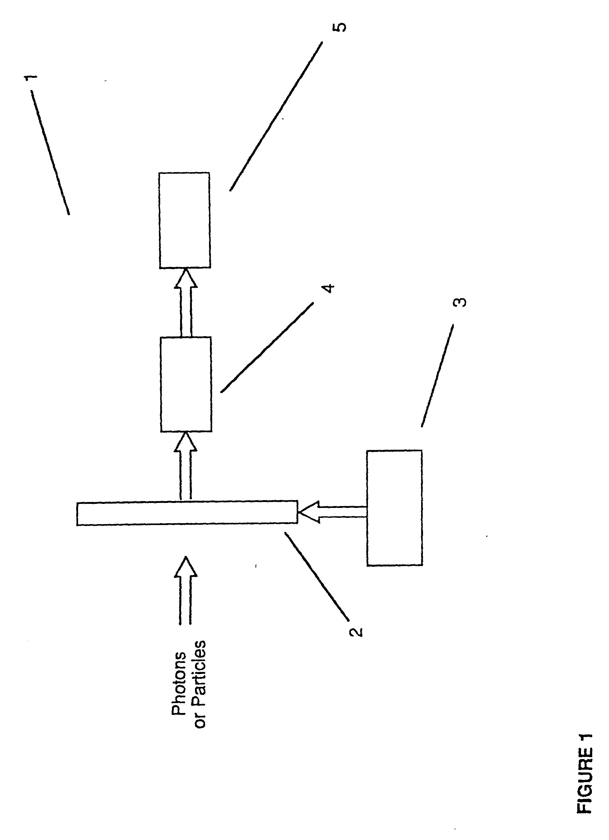
[0022] A preferred embodiment of the present invention, the High Data Rate Smart Sensor System (HDSS) 1 depicted in FIG. 1 block diagram, is designed to processes data generated by an array of detectors located in a sensor 2. This system 1 is further comprised of sensor drive electronics 3. The HDSS may further be comprised of digitizing and output electronics 4, a digital data processor and display 5.

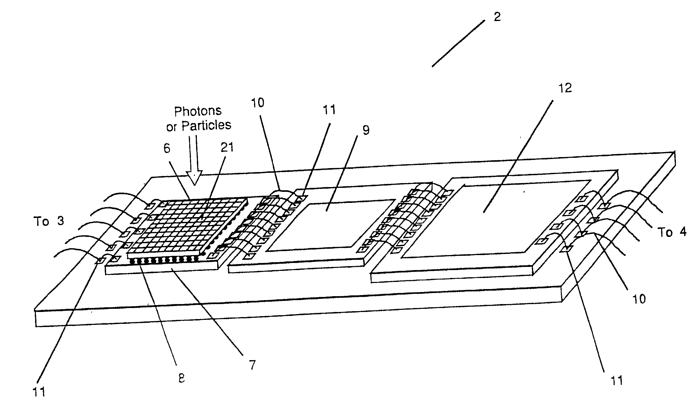
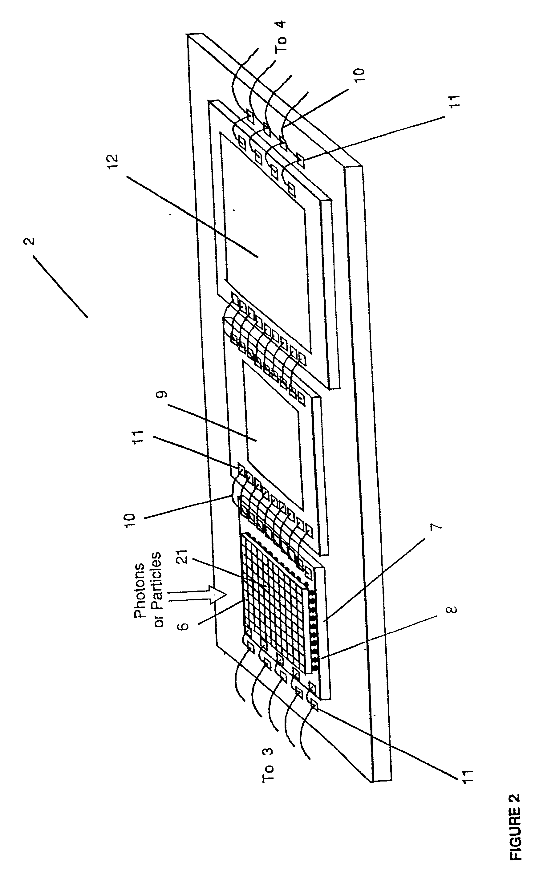
[0023] One embodiment of the sensor 2 is shown in FIG. 2. It is comprised of a detector array chip 6 connected to a readout array chip Z by bump bonds 8; the readout array chip 7 is connected to an analog correction processor 9 by wire bonds 10 and bond pads 11. Typically the detector array is a PIN diode array made from solid-state materials such as silicon or germanium. The readout array chip may be, alternatively, connected to the analog correction processor by a interconnect chip which is bump bonded to both chips; bump bonds taking the place of wire bonds. The analog correction pr...


PUM


Abstract

A device for the high-speed analysis of photon- or particle-generated image data or for the high-speed energy-discrimination analysis of photon- or particle-counting data. A sensor collects the photons or particles on an array of solid state detectors, as electrical analog signals, and stores the analog-signal information on capacitors of readout arrays associated with the detector arrays. Image-related signals are transferred to integrated circuit chips containing an array of correction processor unit cells. Corrected signals are transferred to an analog image processor. Particle-counting data is transferred directly from the readout array chips to the analog image processor having circuitry for implementing an image processing or energy discrimination algorithm.

Description

[0001] analog image processor implements the algorithm and outputs the data in a time frame or less.[0002] Current large detector-array technologies, for particle or photon imaging or for counting, are frame rate or count rate limited. Examples of these detector array technologies are focal plane arrays used for visible and infrared light imaging and detector arrays used for x-ray florescent spectroscopy. The imaging speed limitation is usually related to the need to digitize all the data in the array and transfer it to a digital computer for processing. Digitizing and transferring all the data produces a data rate bottleneck and digitally processing all the data produces a processing rate bottleneck. High frame rates or count rates can currently be handled by massively-parallel digital processors. However, because of the shortcomings of these systems, namely high cost, large size and large-power consumption, this solution is not in common use.[0003] This invention relates to camera...

Claims


Application Information

Patent Timeline
13 Feb 2003
Publication
US20030029989A1
IPC
G01T1/164; G01T1/20; G01T1/24; H01J1/34; H01L27/146; H01L27/148
CPC
G01T1/1644; G01T1/2018; H01J1/34; H01J2201/3423; H01J2231/50031; H01J2231/50063; H01J2231/50068; H01J2231/5056
Inventors
STETTNER, ROGER; BAILEY, HOWARD W.