

Semiconductor integrated circuit
a technology of integrated circuits and semiconductors, applied in the direction of semiconductor/solid-state device testing/measurement, pulse technique, instruments, etc., can solve the problems of test devices, test patterns, and become difficult to carry out tests
- Summary
- Abstract
- Description
- Claims
- Application Information
AI Technical Summary
Problems solved by technology
Method used
Image

Examples
first embodiment
[0020] (First Embodiment)
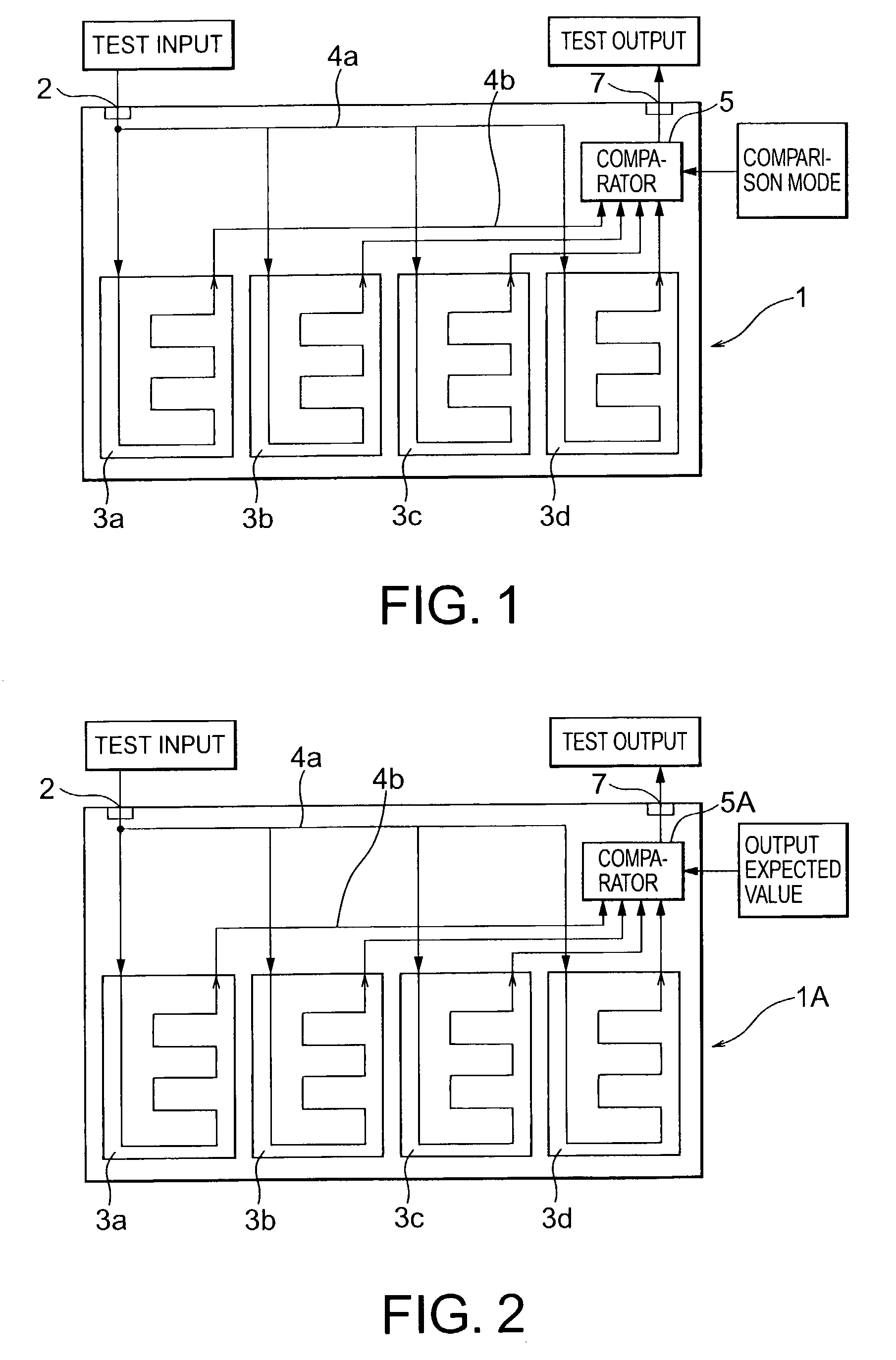
[0021] FIG. 1 shows the structure of a semiconductor integrated circuit according to the first embodiment of the present invention. A semiconductor integrated circuit 1 of this embodiment includes a test input terminal 2, circuits to be tested having the same structure, e.g., logic circuits 3a, 3b, 3c, and 3d, a comparator 5, a test output terminal 7, and test paths 4a and 4b. A test pattern inputted through the test input terminal 2 is sent to each of the logic circuits 3a, 3b, 3c, and 3d via the test path 4a. Further, the test output from each of the logic circuits 3a, 3b, 3c, and 3d is sent to the comparator 5 via the test path 4b. Thus, the test path is branched into paths passing through the logic circuits 3a, 3b, 3c, and 3d.
[0022] The comparator 5 selects whether the test result of any one of the logic circuits 3a, 3b, 3c, and 3d, or the result of comparison of test results of the logic circuits 3a, 3b, 3c, and 3d should be outputted through the test p...
second embodiment
[0026] (Second Embodiment)
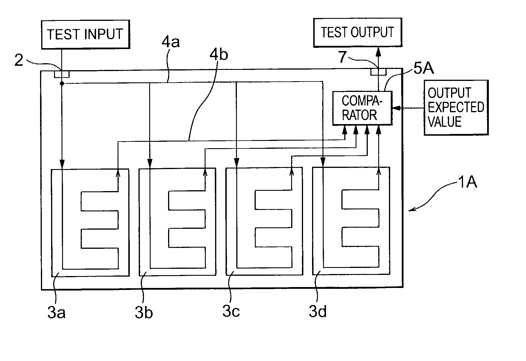
[0027] Next, the structure of a semiconductor integrated circuit according to the second embodiment of the present invention is shown in FIG. 2. A semiconductor integrated circuit 1A of this embodiment is achieved by replacing the comparator 5 of the semiconductor integrated circuit 1 of the first embodiment shown in FIG. 1 with a comparator 5A. The comparator 5A is adjusted to simultaneously compare an inputted output expected value and the test outputs sent from the logic circuits 3a, 3b, 3c, and 3d, to determine whether the inputted output expected value and the test outputs are the same or not, and to output the comparison results. It is possible to carry out the tests of all of the logic circuits 3a, 3b, 3c, and 3d at a time by inputting the test pattern into the comparator 5A at the same time as the test outputs from the logic circuits 3a, 3b, 3c, and 3d are inputted into the comparator 5A. In this way, it is possible to further reduce the time requir...
third embodiment
[0028] (Third Embodiment)
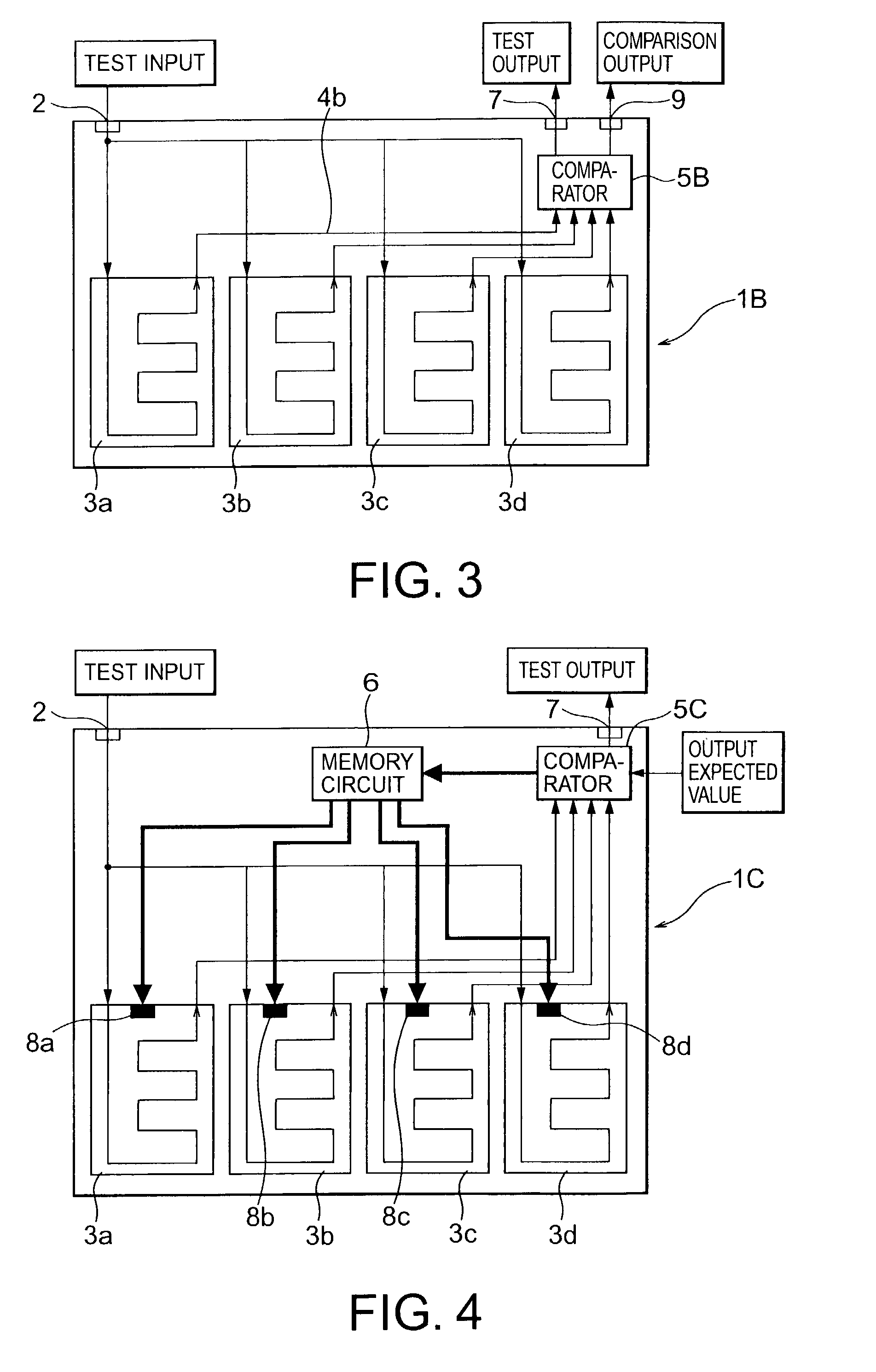
[0029] Next, the structure of a semiconductor integrated circuit of the third embodiment of the present invention is shown in FIG. 3. A semiconductor integrated circuit 1B of this embodiment is achieved by replacing the comparator 5 of the semiconductor integrated circuit 1 of the first embodiment shown in FIG. 1 with a comparator 5B, and by newly adding a comparison output terminal 9. The comparator 5B is configured such that the test path output of a selected one of the logic circuits (the logic circuit 3a in FIG. 3) is outputted from the test output terminal 7 as it is, and that the test outputs of the logic circuits 3a, 3b, 3c, and 3d are simultaneously compared, and the comparison result is outputted to the outside through the comparison output terminal 9.
[0030] In the semiconductor integrated circuit 1B of this embodiment, an external test device compares the test path outputs and the expected value, and also monitors the comparison outputs. Accordingl...
PUM
 Abstract
Description
Claims
Application Information