

Electro-optical device and manufacturing method thereof
a technology of optical devices and optical fibers, applied in the field of semiconductor devices, can solve the problems of deterioration phenomenon that its on-current value falls, high off-current value of polycrystalline silicon tft,
- Summary
- Abstract
- Description
- Claims
- Application Information
AI Technical Summary
Problems solved by technology
Method used
Image

Examples
embodiment 1
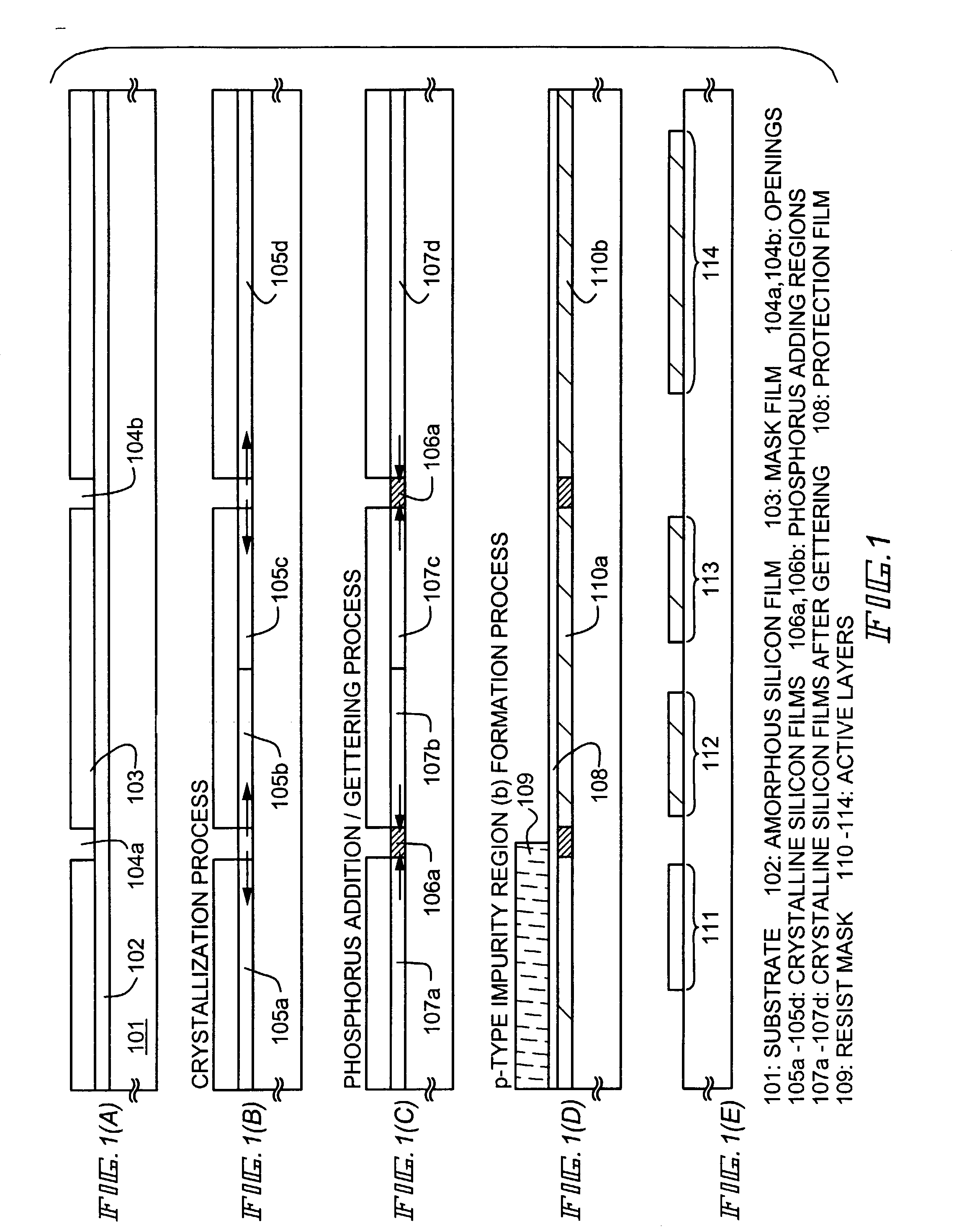
[0063] Embodiment 1
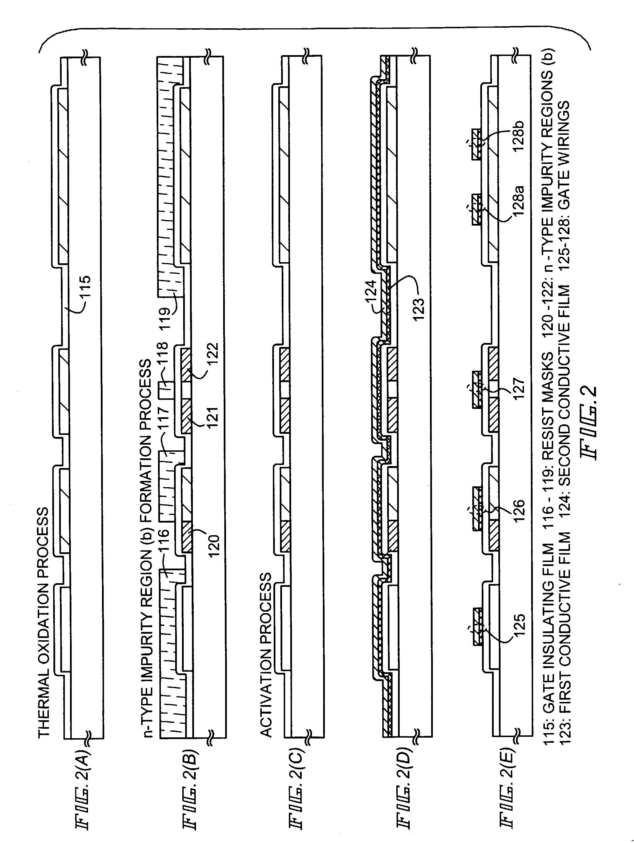
[0064] An Embodiment of the invention will now described refering to FIGS. 1 to 4 Here, the process of simultaneously fabricating a pixel section and a driver circuit for controlling the pixel section over a substrate is described. However, for simplicity of the description, a CMOS circuit that is the basic circuit of a shift register, a buffer, etc., and an n-channel type TFT forming a sampling circuit are shown for the driving circuits.
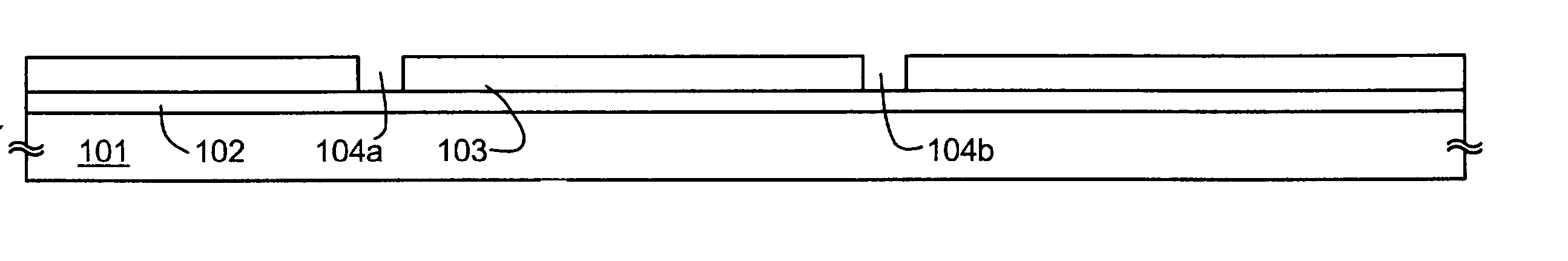
[0065] Referring to FIG. 1A, as a substrate 101, a quartz substrate or a silicon substrate is preferably used. A quartz substrate is used in the present embodiment. Besides, there may also be used a substrate formed with an insulation film on the surface of a metal substrate or a stainless steel substrate. in the case of the present embodiment the heat resistance durable to a temperature exceeding 800.degree. C. is required, and any substrate may be used if the substrate satisfies the heat resistance.
[0066] A semiconductor film 10...
embodiment 2
[0175] Embodiment 2
[0176] The structure of the pixel section that has the structure shown in Embodiment 1 is used by using FIG. 10 in the present embodiment. Note that an arbitrary one pixel in the pixel section is remarked in the top view shown in FIG. 10, and reference numerals used in Embodiment 1 is noted in the same way.
[0177] FIG. 10A is a top view showing the overlap of an active layer, a gate wiring and a source wiring, and FIG. 10B is a top view which shows a state in which a shielding and a pixel electrode is further overlapped thereon. In FIG. 10A, gate wiring 128 intersects an active layer 114 below by interposing a gate insulating film not shown in the figure. Further, though not shown in the figure, a source region, a drain region, a Loft region formed from n-type impurity region (c) are formed in the active layer 114. In addition, 1001 is a contact section of the source wiring 154 and the active layer 114, and 1002 is a contact section of the drain wiring 157 and the ...
embodiment 3
[0180] Embodiment 3
[0181] In the present embodiment a case of differing the structure of the pixel section from Embodiment 2 (refer to FIG. 10) is described by using FIG. 11. Note that the structure of the pixel section described in Embodiments 1 and 2 differ only a part of the gate wiring and are the same structure as a whole. Accordingly, the same reference numerals are used regarding the same section or explain.
[0182] FIG. 11A is a cross sectional diagram of the pixel section of the present embodiment and it is characterized in that a gate wiring (note that the portions overlapping an active layer are excluded) 1101 is formed by laminating a first conductive film 1102, a second conductive film 1103 and a third conductive film 1104. Namely, a structure in which the third conductive film 1104 is sandwiched by the first conductive film 1102 and the second conductive film 1103 is adopted.
[0183] In the present embodiment tantalum nitride film is used as the first conductive film 1102,...
PUM
| Property | Measurement | Unit |
|---|---|---|
| thickness | aaaaa | aaaaa |
| thickness | aaaaa | aaaaa |
| temperature | aaaaa | aaaaa |
Abstract
Description
Claims
Application Information