Three-dimensional optical waveguide, method of manufacturing same, optical module, and optical transmission system

a technology of optical waveguides and optical transmission systems, applied in waveguides, instruments, semiconductor lasers, etc., can solve the problems of increasing cost, difficult spatial adjustment of each waveguide and lens system,

Inactive Publication Date: 2003-08-28
PANASONIC CORP
View PDF17 Cites 82 Cited by
  • Summary
  • Abstract
  • Description
  • Claims
  • Application Information

AI Technical Summary

Problems solved by technology

However, in such a three-dimensional optical waveguide, spatial adjustment in each waveguide and the lens system is extremely difficult.
Therefore, when it is intended to enhance the performance by inserting an optical device such as an isolator in such a three-dimensional optical waveguide, since the number of parts requiring adjustment increases, the cost increases.

Method used


Image

  • Three-dimensional optical waveguide, method of manufacturing same, optical module, and optical transmission system
  • Three-dimensional optical waveguide, method of manufacturing same, optical module, and optical transmission system
  • Three-dimensional optical waveguide, method of manufacturing same, optical module, and optical transmission system

Examples


first embodiment

[0098] (First Embodiment)

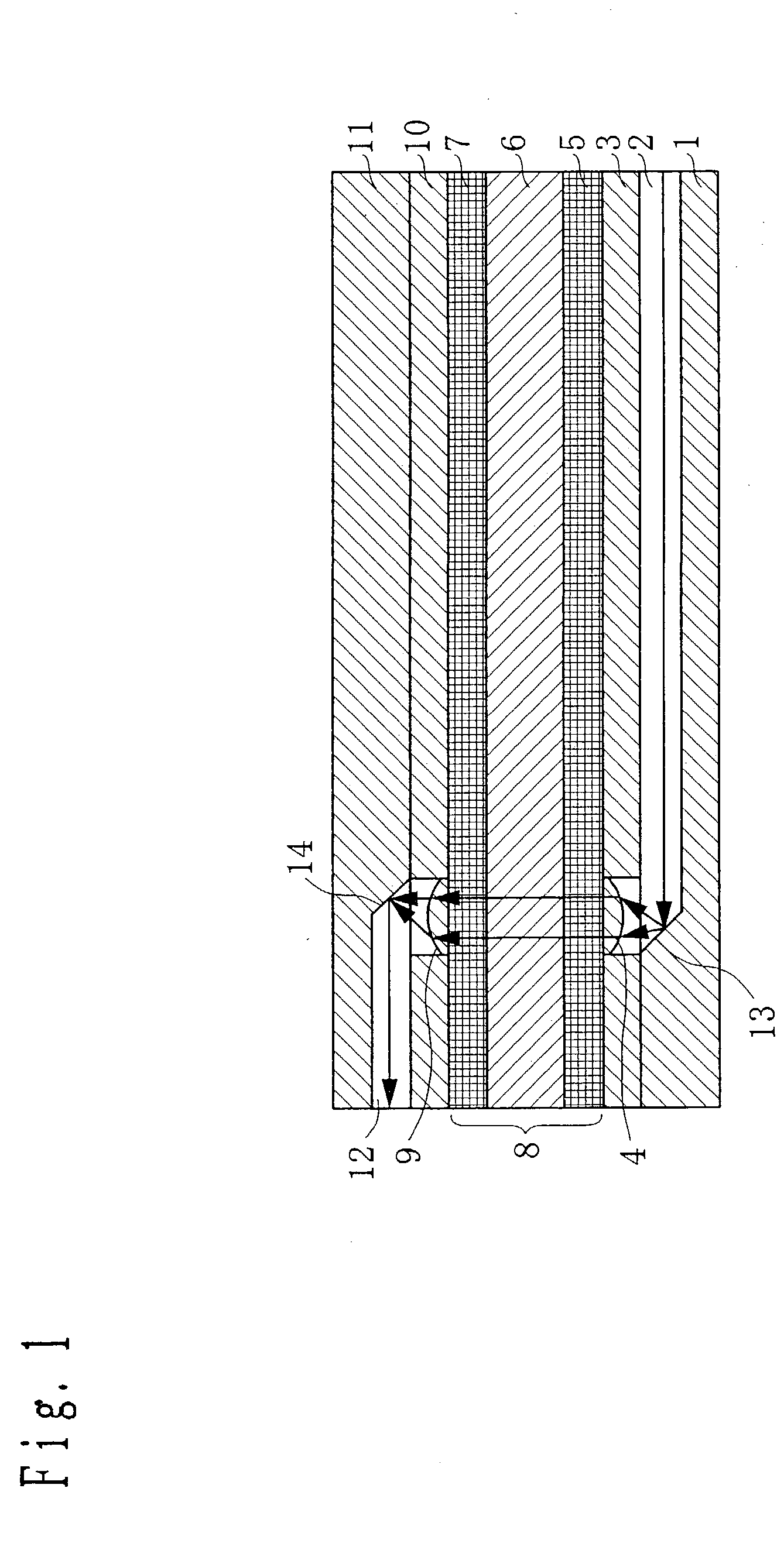
[0099] FIG. 1 shows the cross-sectional structure of a three-dimensional optical waveguide according to a first embodiment of the present invention.

[0100] A waveguide substrate 1 as the planar substrate having a planar waveguide of the present invention is formed of forming glass, and a waveguide 2 which is the planar optical waveguide of the present invention is formed on the top surface of the waveguide substrate 1. At an end of the waveguide 2, a reflecting surface 13 which is the reflecting surface of the present invention comprising a mirror or the like is formed. On the top surface of the waveguide substrate 1, a lens substrate 3 which is the planar substrate having a lens layer of the present invention is laminated. In the lens substrate 3, a lens 4 is integrally formed of forming glass (the same for the lens substrate described below).

[0101] Above the lens substrate 3, a polarizer 5, a Faraday rotator 6 and a polarizer 7 are laminated in this order. ...

second embodiment

[0139] (Second Embodiment)

[0140] Next, a second embodiment of the present invention will be described with reference to FIG. 3.

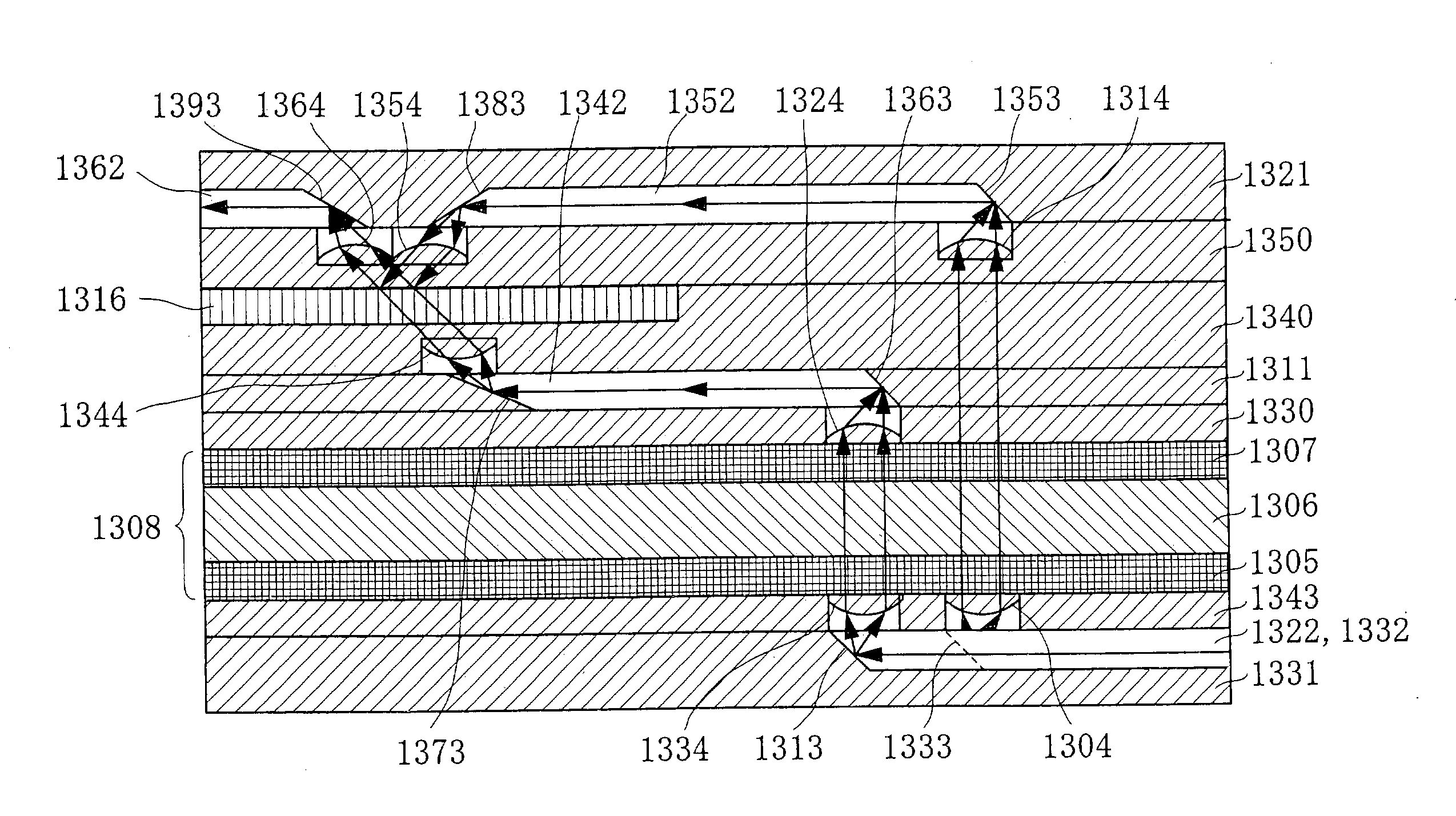
[0141] In the three-dimensional optical waveguide shown in FIG. 3, a waveguide substrate 31 has two waveguides 22 and 32. Here, the waveguide 32 is disposed on the farther side from the plane of FIG. 3 so as to be parallel to the waveguide 22. The waveguide 22 has a reflecting surface 313 at its end, and the waveguide 32 has a reflecting surface 333 at its end. The lens substrate 33 has a lens 34 corresponding to the reflecting surface 313 and a lens 304 corresponding to the reflecting surface 333.

[0142] Above the isolator substrate 8, a lens substrate 30 having a lens 29 corresponding to the lens 34 is laminated, and above the lens substrate 30, a waveguide substrate 31 is laminated having a waveguide 312 and a reflecting surface 314 disposed at an end of the waveguide 312 and corresponding to the lens 29. Above the waveguide substrate 31, a lens substrate ...

third embodiment

[0149] (Third Embodiment)

[0150] FIG. 5 shows the structure of a three-dimensional optical waveguide according to a third embodiment of the present invention.

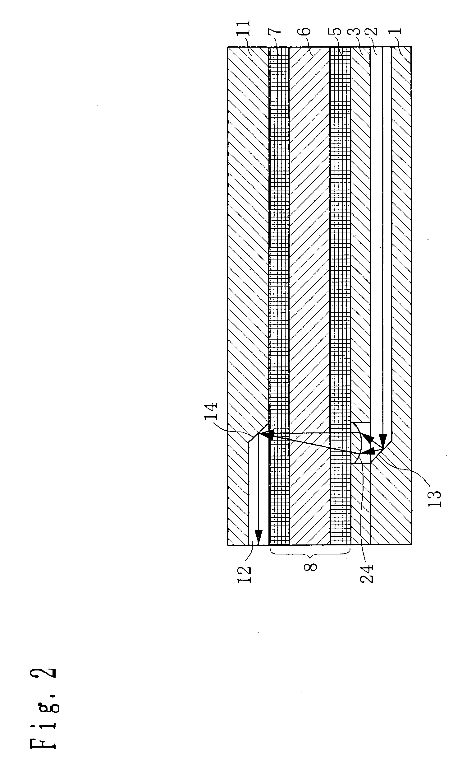
[0151] In the three-dimensional optical waveguide of the present embodiment, a surface emitting laser (VCSEL) 59 which is the light emitting element of the present invention is disposed above the isolator substrate 8, and a reflecting surface 513, a lens 54 and the surface emitting laser 59 are disposed so that the horizontal positions thereof are aligned in the vertical direction. Here, the structure of the part constituted by a waveguide substrate 51, a lens substrate 53 and the isolator substrate 8 is similar to that of the first embodiment, and description thereof is omitted.

[0152] According to the above-described structure, the laser beam emitted from the surface emitting laser 59 passes through the isolator substrate 8 and the lens 54 to be directed to the waveguide 52 of the waveguide substrate 51. By doing this, a low-co...


PUM


Abstract

A three-dimensional optical waveguide is formed by laminating planar substrates such as a plurality of lens substrates and, an isolator substrate and a wavelength division multiplexing filter, the optical substrates at least include a waveguide substrate having a waveguide and a reflecting surface. In the three-dimensional optical waveguide, the planar substrates are positioned by markers integrally formed on at least two of the planar substrates. Light directed into the waveguide is reflected by a reflecting surface and passes through the lens substrates and the isolator substrate.

Description

[0001] 1. Field of the Invention[0002] The present invention relates to a three-dimensional optical waveguide, a method of manufacturing the same, an optical module, and an optical transmission system for enhancing the performance of an optical device.[0003] 2. Related Art of the Invention[0004] Conventionally, when a three-dimensional optical waveguide is formed, for example, in order that light traveling through a waveguide is output vertically with respect to the waveguide, as shown in FIG. 26, a planar filter 1006 such as a wavelength division multiplexing (WDM) filter is inserted in a groove 1002 obliquely formed in a planar waveguide 1001, and the light reflected or transmitted by the planar filter 1006 is oriented with respect to a light receiving element 1008, a lens system and another planar optical waveguide which are disposed spatially, thereby forming the three-dimensional optical waveguide.[0005] However, in such a three-dimensional optical waveguide, spatial adjustment...

Claims


Application Information

Patent Timeline
Patent Type & Authority Applications(United States)
IPC IPC(8): G02B6/12G02B6/122G02B6/42G02B6/43H01L31/12H01S5/026
CPCG02B6/12002G02B6/43G02B6/4214G02B6/4204Y10S385/901
Inventor ISHIDA, KAORUKORENAGA, TSUGUHIRO
Owner PANASONIC CORP
Why Eureka
Try Eureka