Method of forming resist pattern
- Summary
- Abstract
- Description
- Claims
- Application Information
AI Technical Summary
Problems solved by technology
Method used
Image

Examples
first embodiment
[0053] A method of forming a resist pattern according to a first embodiment of the invention is shown in FIGS. 3A and 3B. FIG. 3A shows the state before a reflowing process and FIG. 3B shows the state after the reflowing process.
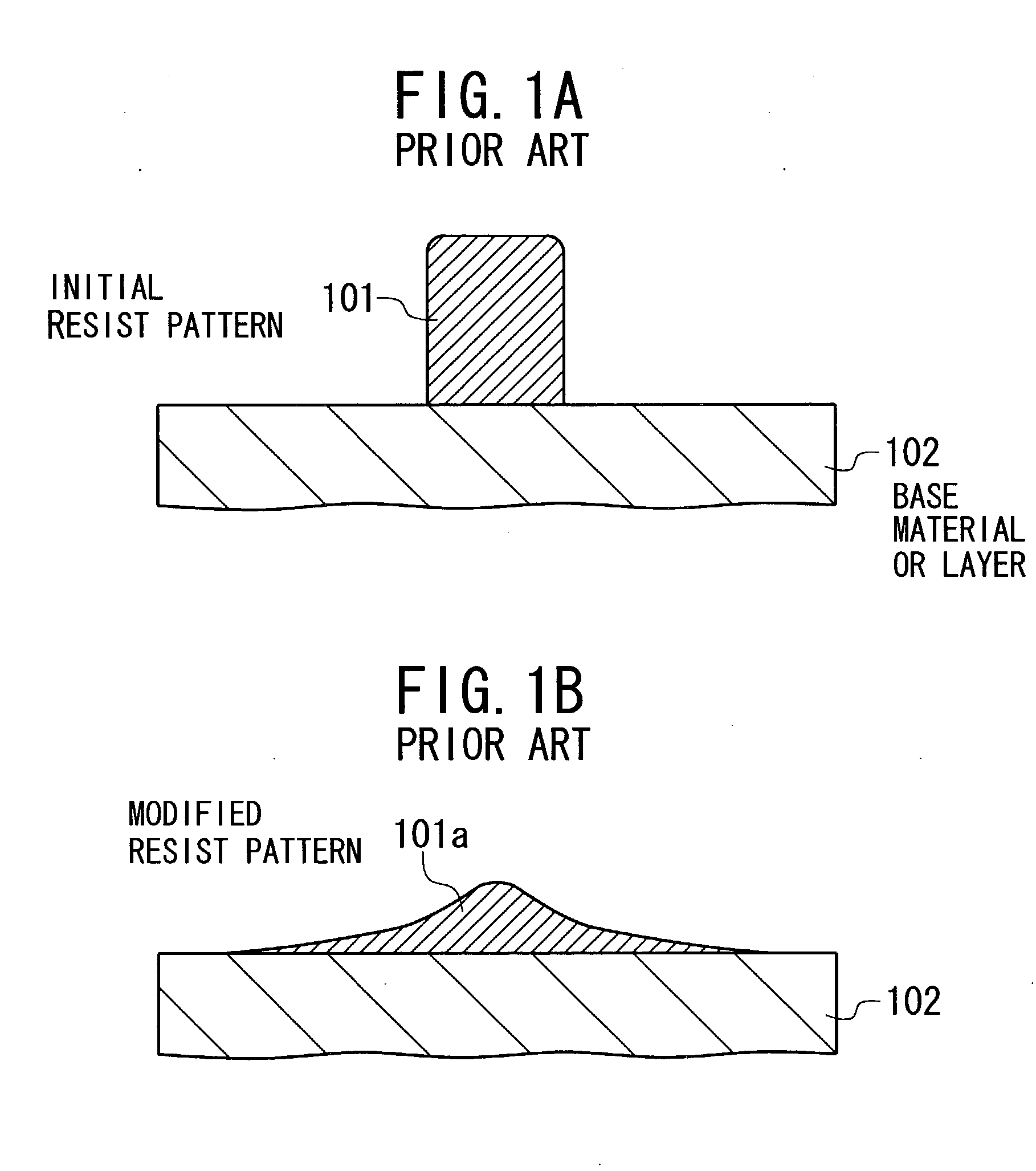
[0054] First, as shown in FIG. 3A, an initial resist pattern 1 with a specific shape is formed on a base material or layer 2 by a known method. This pattern 1 is used as a mask for a first etching process.
[0055] Next, a surface treatment is carried out to adjust the "wettability" of the exposed surface 3 of the underlying base material or layer 2. Thus, the wettability of the exposed surface 3 is adjusted, in other words, the wettability of the exposed surface 3 is decreased or increased according to the necessity. The state at this stage is shown in FIG. 3A.
[0056] Generally, whether the wettability of a surface is good or bad is evaluated by using a "contact angle". Here, the "contact angle" of a liquid drop contacting the surface of a solid at a contact po...
second embodiment
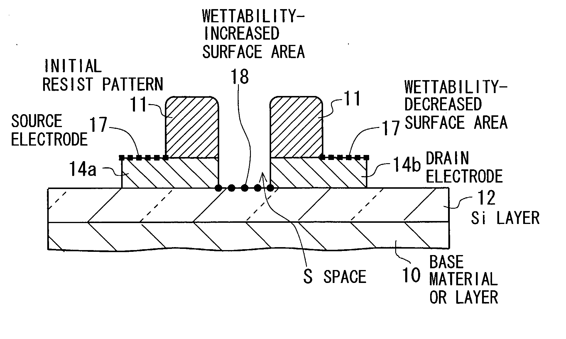
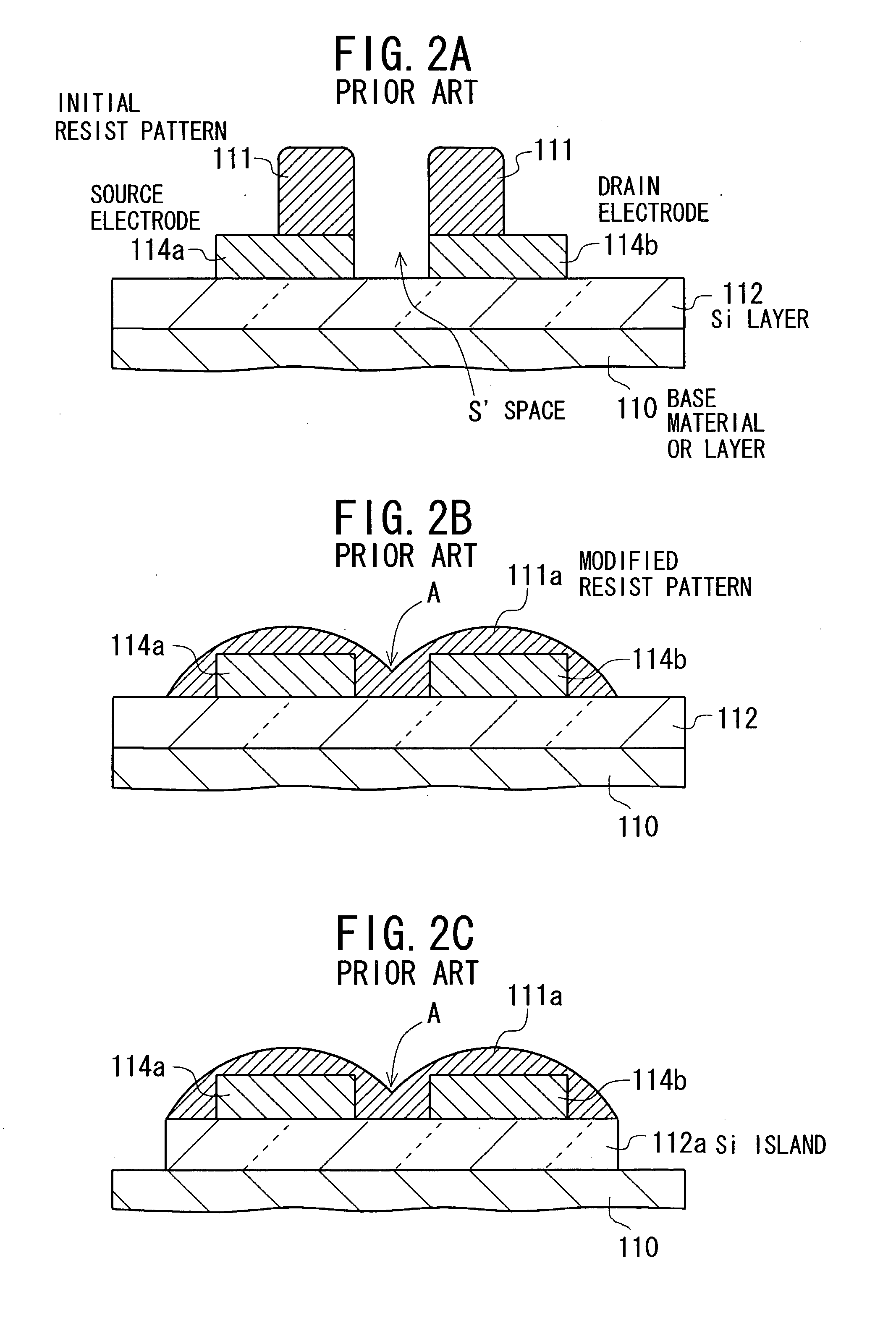
[0067] FIGS. 4A to 4C show a method of forming a resist pattern according to a second embodiment of the invention, in which the method of the first embodiment is applied to the fabrication of a FET. FIG. 4A shows the state after the first etching process and before a reflowing process, FIG. 4B shows the state after the reflowing process, and FIG. 4C shows the state after the second etching process.
[0068] First, as shown in FIG. 4A, a single-crystal or polycrystalline Si layer 12 is formed on a base material or layer 10. A source electrode 14a and a drain electrode 14b are formed on the Si layer 12 to be apart from each other at a distance, forming a space S between the electrodes 14a and 14b. These electrodes 14a and 14b are formed by patterning a Cr layer.
[0069] An initial resist pattern or a patterned resist layer 11 is formed on the source and drain electrodes 14a and 14b. This pattern 11 is obtained by narrowing the width of its original resist pattern (not shown) for forming th...
PUM
 Abstract
Description
Claims
Application Information