Method and apparatus for mapping memory addresses to corresponding cache entries

a memory address and cache entry technology, applied in the field of cache memory design, can solve the problems of increasing pressure on computer system designers to achieve shorter propagation delays through computational circuitry, memory access delays can generate a severe bottleneck, and the computational performance depends on not only the processor speed, but also other time-consuming operations

Active Publication Date: 2004-11-11
ORACLE INT CORP
View PDF4 Cites 14 Cited by
  • Summary
  • Abstract
  • Description
  • Claims
  • Application Information

AI Technical Summary

Problems solved by technology

As processor clock speeds continue to increase at an exponential rate, computer system designers are under increasing pressure to achieve shorter propagation delays through computational circuitry.
Unfortunately, computational performance depends on not only processor speed, but also other time-consuming operations.
In particular, memory access delays can generate a severe bottleneck as processor speeds reach beyond multiple gigabits per second.
However, a cache memory cannot be made infinitely large because of chip area and timing constraints.
Otherwise, a cache miss occurs and the processor stalls to wait for a memory access.
In designing a cache memory, one challenge is to minimize cache misses and to achieve a more uniform cache-access pattern.
Existing cache mapping schemes are far from perfect.
It has been observed that frequently accessed data items are often mapped to the same cache entries, which causes frequent cache line evictions and cache misses.
As a result, some cache entries suffer more misses than others do.
However, these solutions each have trade-offs in increased cost and complexity.
Great ingenuity, expense, and effort have gone into solving the non-uniform cache miss problem; nevertheless, the results have so far been unsatisfactory.

Method used


Image

  • Method and apparatus for mapping memory addresses to corresponding cache entries
  • Method and apparatus for mapping memory addresses to corresponding cache entries
  • Method and apparatus for mapping memory addresses to corresponding cache entries

Examples


Embodiment Construction

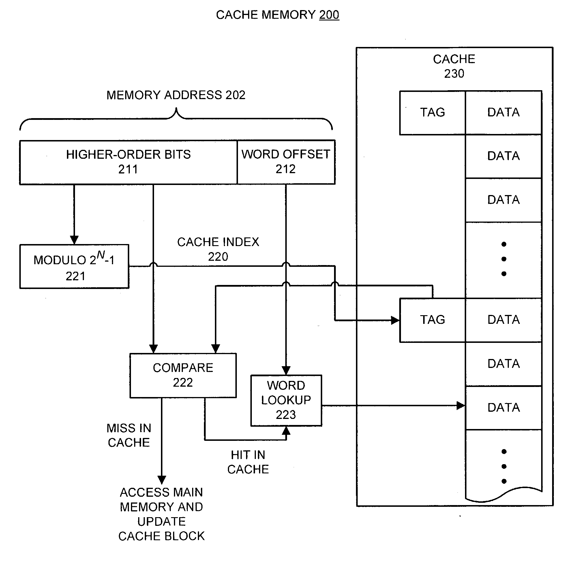
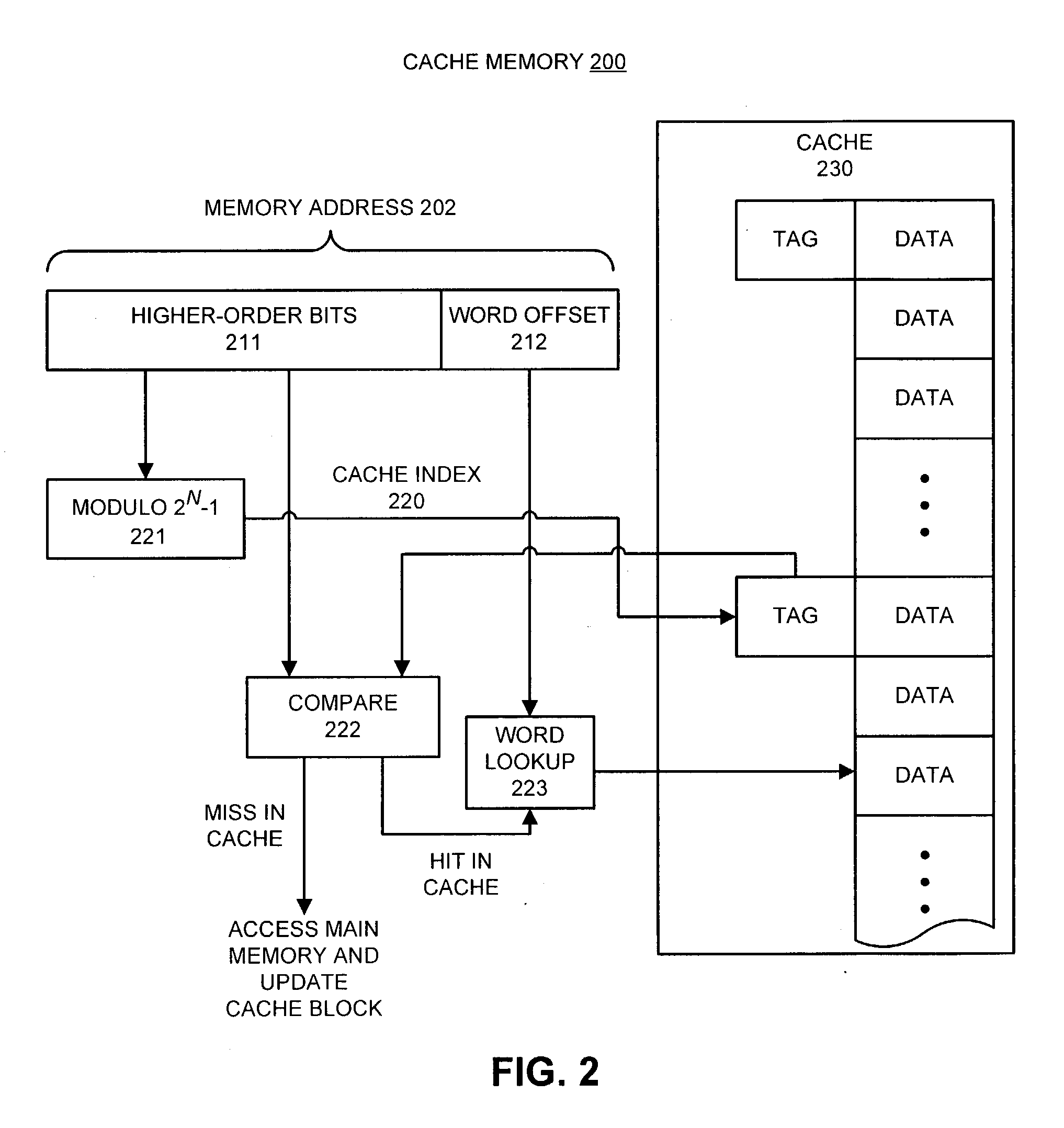
[0049] Table 1 presents exemplary C code illustrating how the hardware 10 in one embodiment of the present invention calculates the (2.sup.N-1) modulo of the higher-order bits of a memory address for an exemplary 8 MB direct-mapped cache with 64 byte blocks.

1TABLE 1 #define CACHE_BLOCK_ADDR_BITS 6 / * 26{circumflex over ( )}6 = 64 bytes * / #define CACHE_ENTRIES_MASK 0x1ffff / * 2{circumflex over ( )}17-1 * / #detine CACHE_ENTRY_BITS 17 / * 2{circumflex over ( )}17 = 8 MB * / cacheIndex (paddr) { / * assumes 40 bit paddr* / paddr=paddr>>CACHE_BLOCK_ADDR_B-ITS; do{ paddr = (paddr&CACHE_ENTRIES_MASK) + ((paddr>>CACHE_ENTRY_BITS)& CACHE_ENTRIES_MASK); }while(paddr>CACHE_ENTRIES_MASK); return paddr==CACHE_ENTRIES_MASK ? 0 : paddr; }

[0050] In another embodiment of the present invention, the system can simplify the (2.sup.N-1) modulo operation as is illustrated by the C code shown in Table 2.

2TABLE 2 #define CACHE_BLOCK_ADDR_BITS 6 / * 2{circumflex over ( )}6 = 64 bytes * / #define CACHE_ENTRIES_MA...


PUM


Abstract

One embodiment of the present invention provides a system for mapping memory addresses to cache entries. The system operates by first receiving a memory request at the cache memory, wherein the memory request includes a memory address. The system then partitions the memory address into a set of word offset bits and a set of higher-order bits. Next, the system maps the memory address to a cache entry by computing a modulo operation on the higher-order bits with respect to an integer and using the result as the cache index.

Description

[0001] This application hereby claims priority under 35 U.S.C. .sctn.119 to U.S. Provisional Patent Application No. 60 / 468,571, filed on 6 May 2003, entitled "Efficient Mapping of Physical Memory to Cache Blocks," by inventor Robert M. Lane.[0002] 1. Field of the Invention[0003] The present invention relates to the design of cache memories within computer systems. More specifically, the present invention relates to a method and apparatus for mapping memory addresses to corresponding cache entries.[0004] 2. Related Art[0005] As processor clock speeds continue to increase at an exponential rate, computer system designers are under increasing pressure to achieve shorter propagation delays through computational circuitry. Unfortunately, computational performance depends on not only processor speed, but also other time-consuming operations. In particular, memory access delays can generate a severe bottleneck as processor speeds reach beyond multiple gigabits per second.[0006] A common te...

Claims


Application Information

Patent Timeline
Patent Type & Authority Applications(United States)
IPC IPC(8): G06F12/08
CPCG06F12/0864
Inventor LANE, ROBERT M.
Owner ORACLE INT CORP
Why Eureka
Try Eureka