

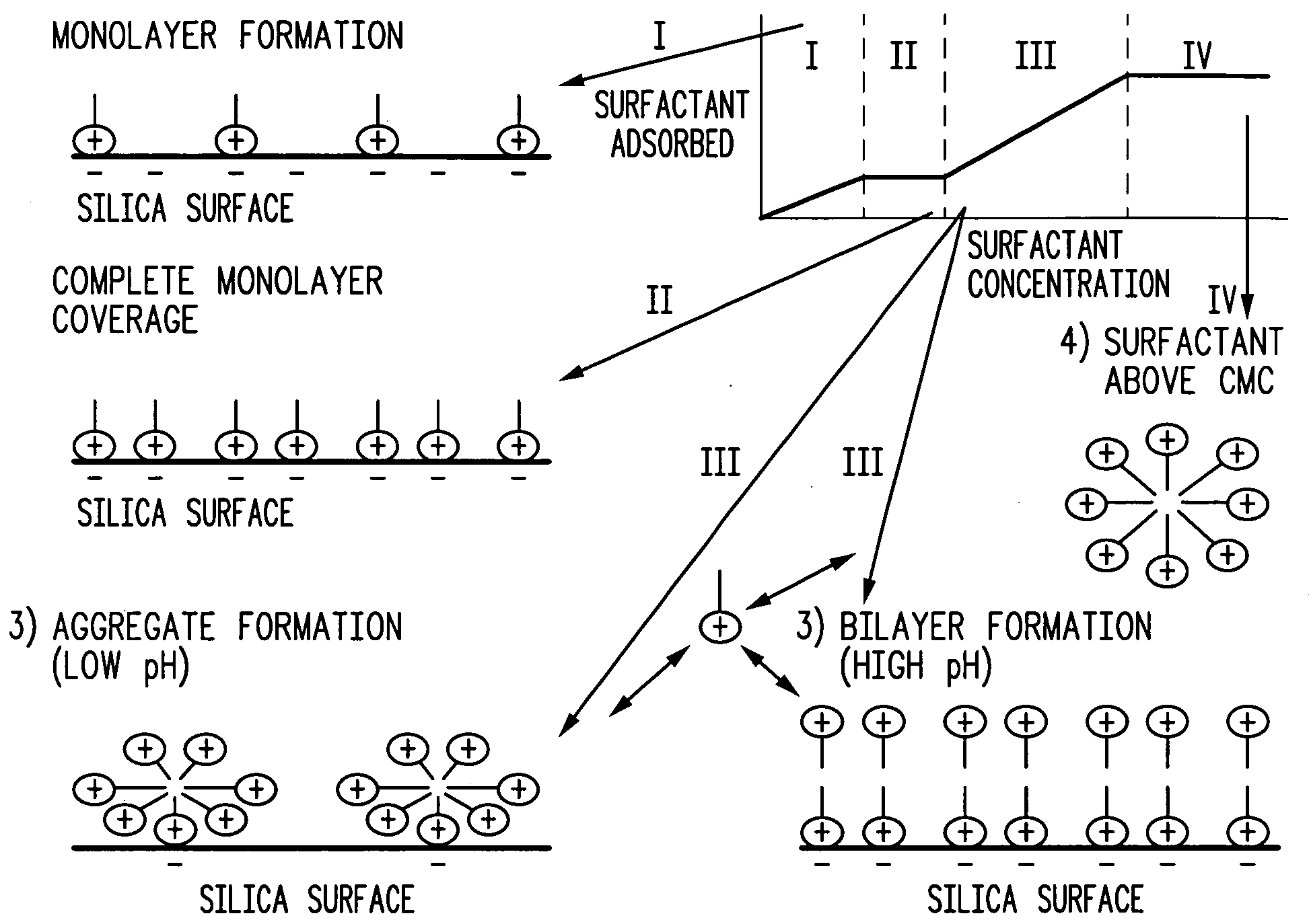
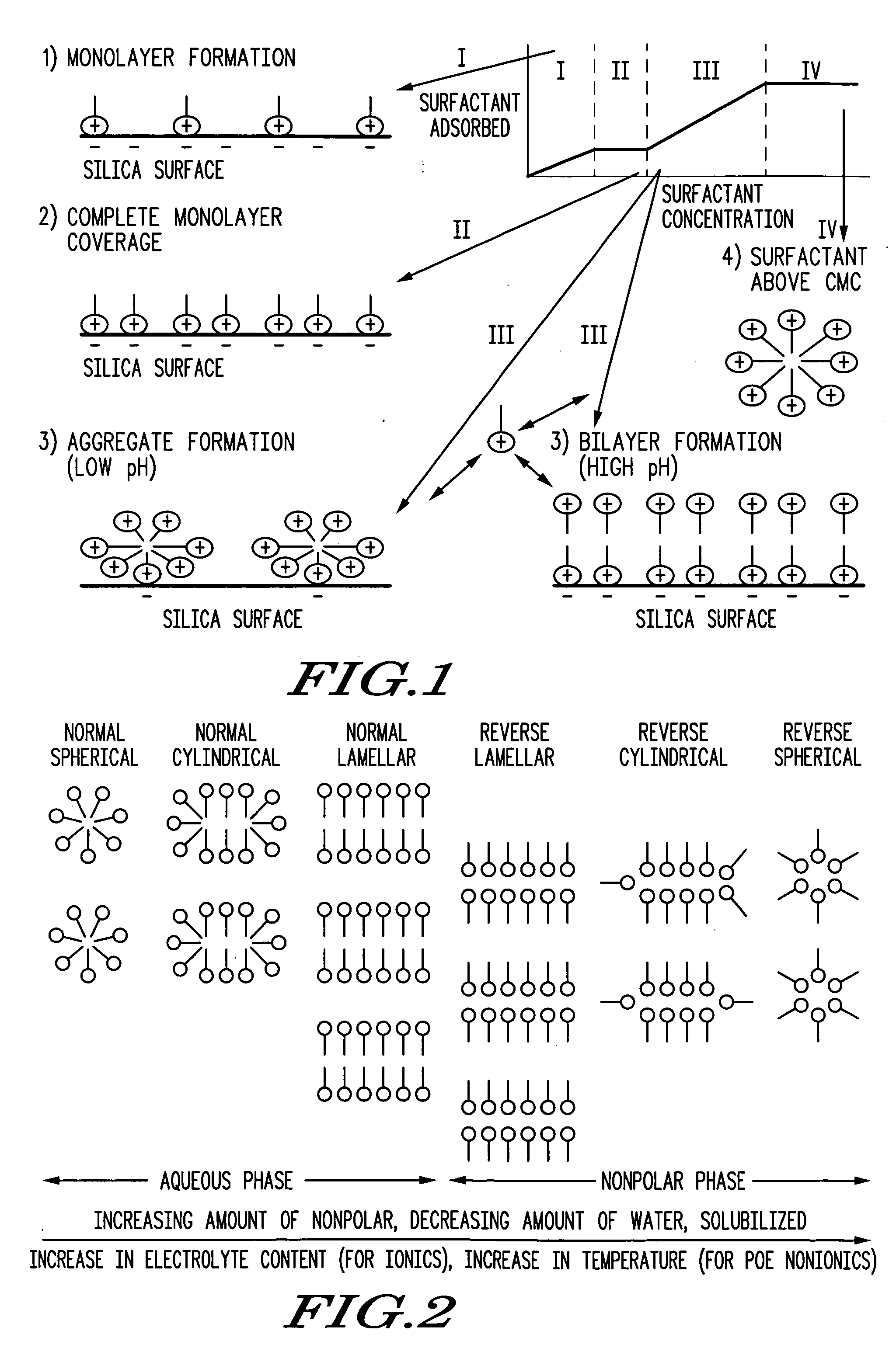
Micellar technology for post-etch residues
a technology of micellar technology and post-etch residues, which is applied in the field of micellar technology for post-etch residues, can solve the problems of low device yield, high via resistance, and voids in the via
- Summary
- Abstract
- Description
- Claims
- Application Information
AI Technical Summary
Problems solved by technology
Method used
Image

Examples
examples 1-5
utilized five different aqueous, micellar solutions based on the surfactants listed in TABLE 1. In each solution, the concentration of the surfactant was adjusted to 0.1%. EGMBE was used as a 5% solution, whereas citric acid and oxalic acid were used as 3% solutions. These micellar solutions were then used to clean die of the type used in COMPARATIVE EXAMPLE 1 in a post-etch process. After the die were cleaned and dried, the Kelvin contact resistance of the wafers was determined following the same procedures as used in COMPARATIVE EXAMPLE 1. The results are depicted graphically in FIG. 5 and are also set forth in TABLE 1.
As indicated by the results shown in FIG. 5 and TABLE 1, the use of a micellar solution in cleaning the vias had a dramatic affect on Kelvin contact resistance in some instances. Thus, while the baseline process of COMPARATIVE EXAMPLE 1 gave rise to a Kelvin contact resistance of about 1.7 ohms / contact, the Kelvin contact resistance of wafers cleaned with the micel...
examples 6-10
These examples illustrate the improvements possible in contact resistance and yield through the use of micellar cleaning solutions on die containing large via structures.
In EXAMPLES 6-10, six aqueous, micellar solutions were prepared based on the surfactants listed in TABLE 2. In each solution, the concentration of the surfactant was adjusted to 0.1%. EGMBE was used as a 5% solution, whereas citric acid and oxalic acid were used as 3% solutions. These micellar solutions were then used to clean die of the type used in COMPARATIVE EXAMPLE 2. After the die were cleaned and dried, the contact resistance of the wafers was determined. The results are depicted graphically in FIG. 7 and are summarized in TABLE 2. The number of die used in each experiment is also indicated in TABLE 2.
TABLE 2Via Chain Yields on BE836.1 Zig-Zag DieExampleVia Chain YieldNo.Surfactant Identity(%)C-2None63E-6FSA + DHF100E-7FSB63E-8EGMBE100E-9Ashland Surfactant ®100E-10Oxalic acid100
As shown by the data in T...
examples 11-21
These examples illustrate the improvements possible in contact resistance and via chain yield through the use of micellar cleaning solutions on wafers have a large number of vias.
COMPARATIVE EXAMPLES 3-5 were repeated, except this time the vias in the die were cleaned with the micellar solutions indicated in TABLE 3. The results are depicted graphically in FIGS. 8-10 and are summarized in TABLE 3.
As the results indicate, the use of certain micellar solutions affords dramatic increases in via chain yields. The micellar solutions of EXAMPLES 11-13 were especially effective and were seen to give via chain yields of about 90-96%, far above the yields afforded by the baseline process. The micellar solutions of EXAMPLES 14-15 also provided dramatically improved via chain yields (70-78%).
TABLE 3Via Chain Yields on BE836 DieVia ZigzagExampleSurfactantSurfactantArrayVia ChainNo.No.IdentityLocationYield (%)C-2NoneNone863.1 C115C-3NoneNone863.1 C225C-4NoneNone863.2 C222E-11S1Ashland863....
PUM
 Abstract
Description
Claims
Application Information