MEMS having a three-wafer structure

a technology of mechanical structure and three-wafer, which is applied in the direction of snap-action arrangement, instruments, and mechanical/solid-state device details, etc., can solve the problems of difficult to restrict the movement of the mechanical structure to the desired plane, mechanical structure suffers from performance limitations, and transducers have very limited application

Inactive Publication Date: 2005-02-03
HEWLETT PACKARD DEV CO LP
View PDF20 Cites 21 Cited by
  • Summary
  • Abstract
  • Description
  • Claims
  • Application Information

AI Technical Summary

Problems solved by technology

Because of the limited thickness of the mechanical structure, the mechanical structure suffers from performance limitations.
For example, because of the minimal thickness of the mechanical structure it is difficult to restrict the movement of the mechanical structure to the desired plane.
Due to crosstalk, resulting from the single-wafer MEMS structure, these transducers have very limited application.
This results in performance degradation and increased costs.
Also, these two chips must be packaged together as a single device, which increases costs.

Method used


Image

  • MEMS having a three-wafer structure
  • MEMS having a three-wafer structure
  • MEMS having a three-wafer structure

Examples


Embodiment Construction

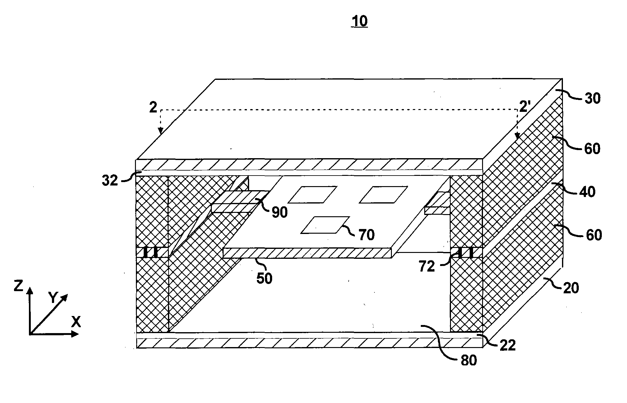
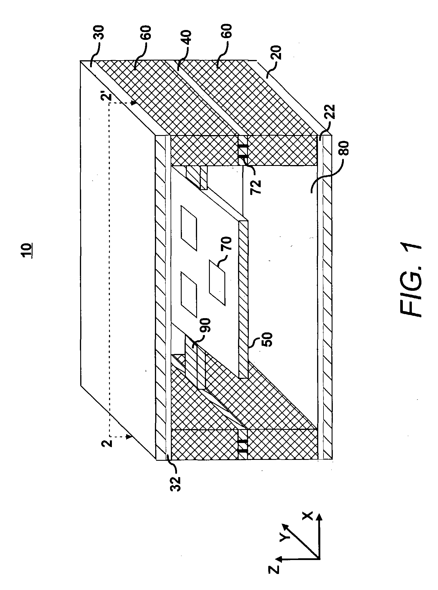
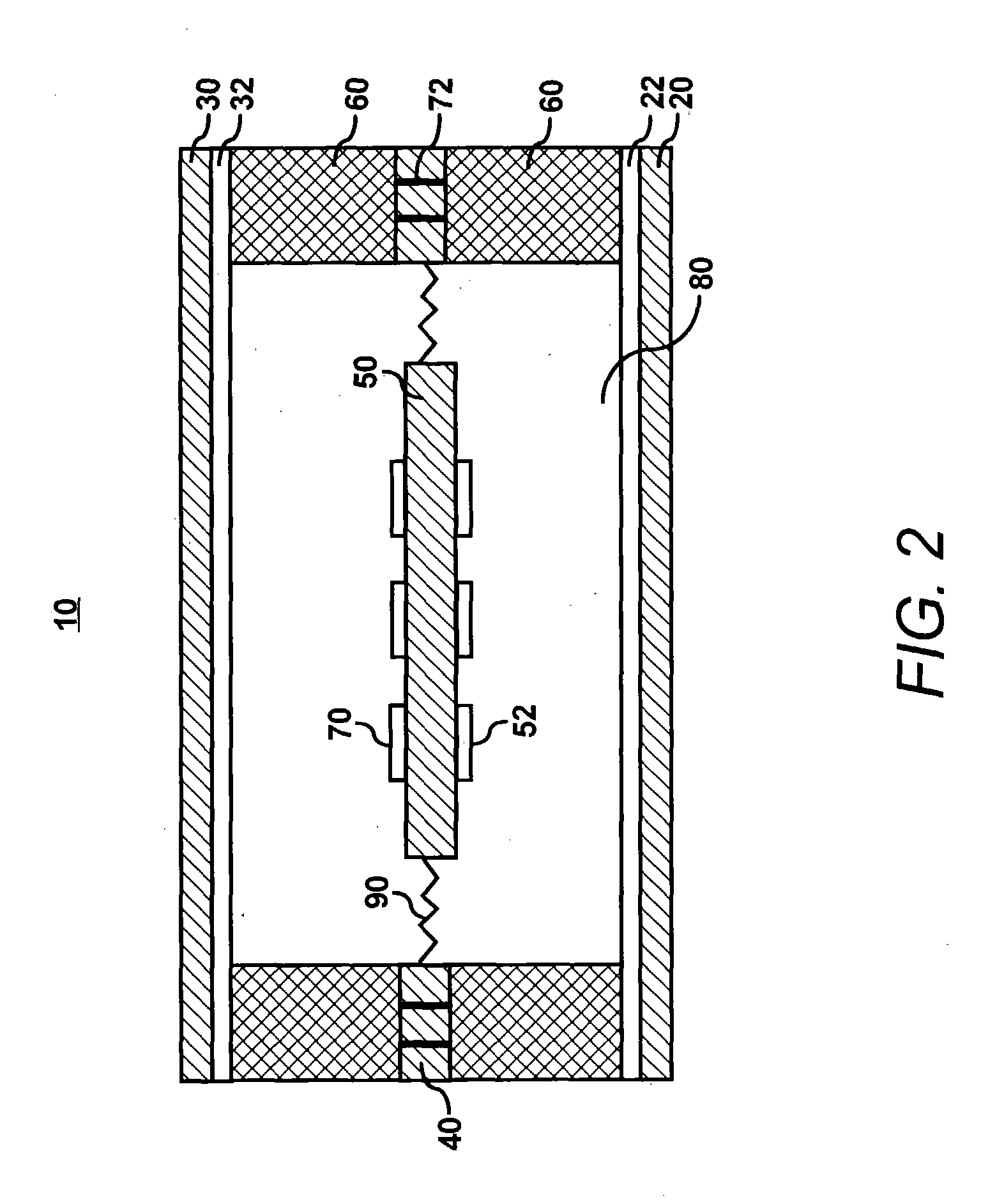
[0005] According to an embodiment, a microelectromechanical system (MEMS) device comprises a first wafer, a second wafer, and a third wafer. At least a portion of the second wafer is movably connected between the first wafer and the third wafer. A material is included that bonds the first wafer, the second wafer, and the third wafer together.

[0006] According to another embodiment, a MEMS device comprises a chip including three wafers connected together in a stacked arrangement. The stacked arrangement comprises a first wafer of the three wafers, a second wafer of the three wafers connected below the first wafer in the stacked arrangement wherein the second wafer includes a movable portion, and a third wafer of the three wafers connected below the second wafer in the stacked arrangement. The three wafers are connected using a bonding material. At least one via in the second wafer is provided that is operable to pass electrical signals through the second wafer.

[0007] According to an...


PUM


Abstract

A microelectromechanical system includes a first wafer, a second wafer including a moveable portion, and a third wafer. The movable portion is movable between the first wafer and the third wafer. The first wafer, the second wafer, and the third wafer are bonded together.

Description

FIELD OF THE INVENTION [0001] This invention relates generally to a microelectromechanical system (MEMS). More particularly, the invention relates to microelectromechanical system having a three-wafer structure. BACKGROUND OF THE INVENTION [0002] MEMS devices are a combination of micro mechanical and micro electronic systems that are revolutionizing nearly every product category by bringing together these systems. A MEMS device typically comprises a movable micro mechanical structure and silicon based microelectronics. One type of known MEMS device is a MEMS transducer. Analog Devices™ manufactures a capacitive MEMS transducer used in an air-bag system for crash detection. For example, a crash is detected by monitoring the movement of the mechanical structure in the MEMS transducer using associated microelectronics in the MEMS transducer. The mechanical structure in the transducer comprises a capacitive plate which is relative to another capacitive plate in the transducer. As the me...

Claims


Application Information

Patent Timeline
Patent Type & Authority Applications(United States)
IPC IPC(8): G01P15/125B81B3/00B81B5/00B81B7/00B81B7/02H01L29/82H01L33/00
CPCB81B7/0041B81C2203/019B81C2201/019B81B2201/0235G01P2015/082
Inventor HARTWELL, PETER G.HOEN, STORRS T.HORSLEY, DAVIDYANG, CHUNG CHINGMERCHANT, PAUL P.TAUSSIG, CARL P.O'NEILL-MERCHANT, GAIL
Owner HEWLETT PACKARD DEV CO LP
Why Eureka
Try Eureka