
Light-emitting device including a dual emission panel

Inactive Publication Date: 2005-02-03
SEMICON ENERGY LAB CO LTD
View PDF21 Cites 39 Cited by
  • Summary
  • Abstract
  • Description
  • Claims
  • Application Information

AI Technical Summary

Benefits of technology

[0009] In the view of the foregoing, it is an object of the present invention to provide a light-emitting device by which an erect image and an external image can be seen simultaneously, and a light-emitting device by which erect images can be simultaneously seen on both surfaces of the light-emitting device.

Problems solved by technology

There is a problem in a light-emitting device emitting light out of both surfaces that an image on the surface and an image on the rear surface are different from each other (either image is mirror-reversed), and so erect images cannot be simultaneously seen on both surfaces.

Method used


Image

  • Light-emitting device including a dual emission panel
  • Light-emitting device including a dual emission panel
  • Light-emitting device including a dual emission panel

Examples


example 1

[0028] In Example 1, a specific example of a display device explained in Embodiment is explained with reference to FIGS. 2 to 4C.

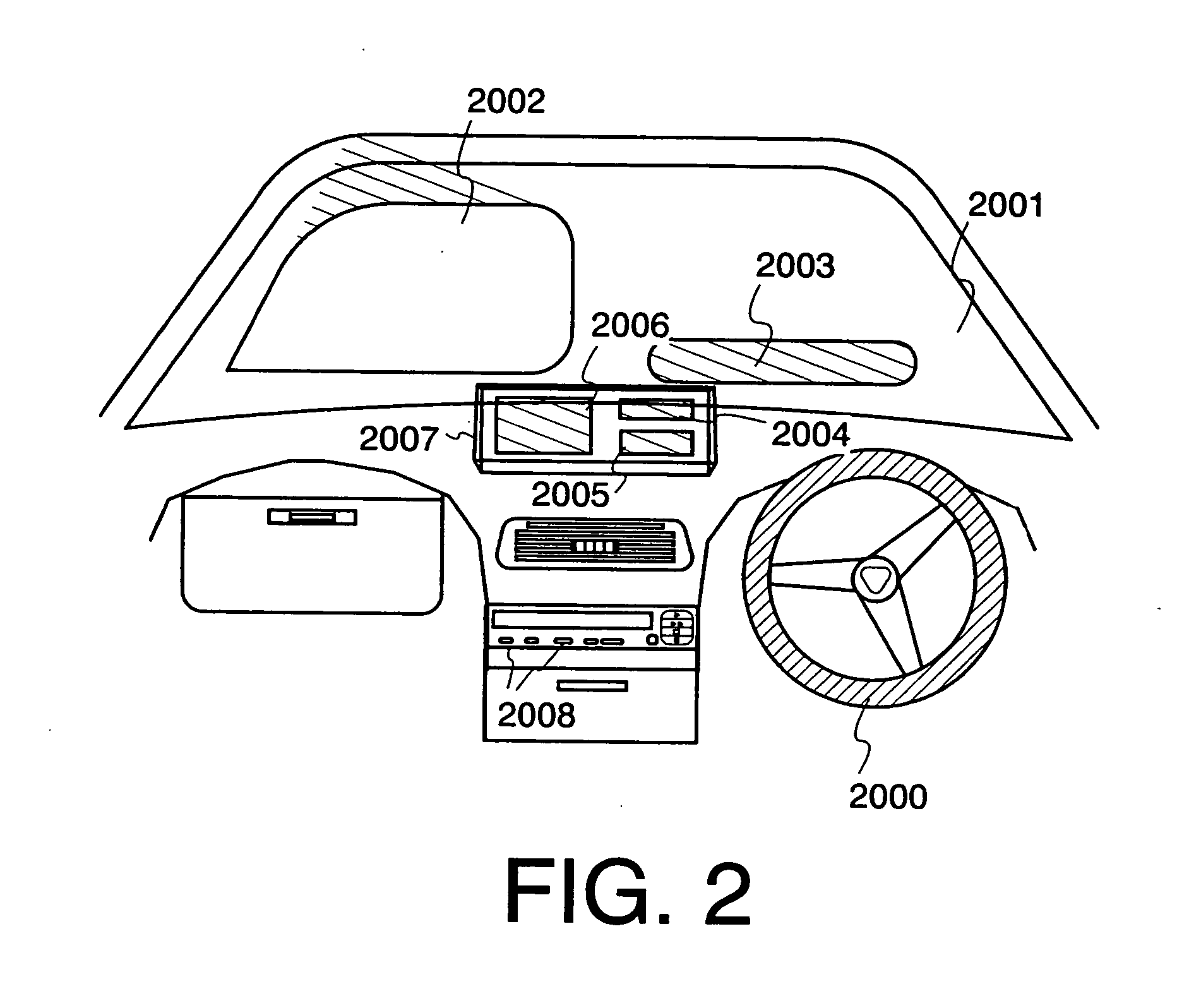
[0029]FIG. 2 shows an example in which a front glass is used in a vehicle as a display device. FIG. 2 is an internal view of a vehicle. Reference numeral 2000 denotes a handle; 2001, a front glass; 2007, an interior; and 2008, operation buttons. A display device according to the invention is provided to the interior 2007. Images are displayed on screens of a display portion A 2002, a display portion B 2003, a display portion C 2004, a display portion D 2005, and a display portion E 2006. Further, the front glass 2001 corresponds to the support 24 described in Embodiment.

[0030] A light-emitting device included in the interior 2007 is a dual emission device. The dual emission device and the front glass 2001 compose the structure explained in Embodiment. A light-emitting device is capable of dual emission. Light emitted from the opposite side of a driver is...

example 2

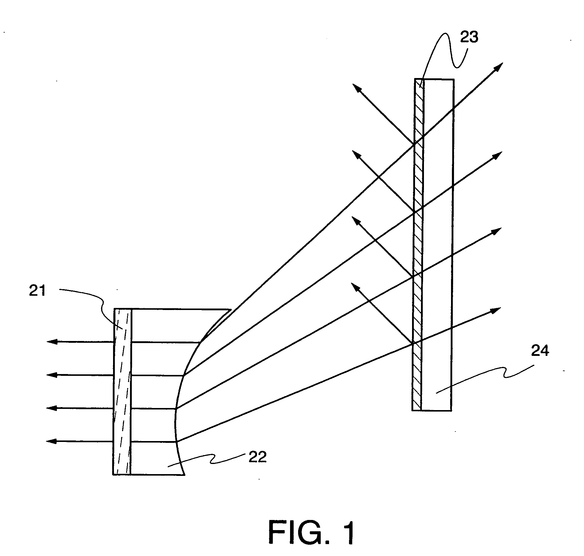
[0045] An example of a structure in which a reverse image from a light-emitting device 21 is projected on a semi-transmissive film 23 via one optical device 22 is explained in Example 1. Alternatively, a structure in which a plurality of optical devices such as mirrors is sandwiched between the light-emitting device and the semi-transmissive film can be adopted. The structure is explained hereinafter with reference to FIGS. 7A and 7B.

[0046]FIG. 7A shows a structure in which three mirrors 72, 73, and 74 are sandwiched between a light-emitting device 71 and a semi-transmissive film 75. The number of mirrors is not limited to three as long as it is an odd number. Since an image obtained from one side of the light-emitting device 71 (left side in FIG. 7A) is an erect image, and an image obtained from another side (right side in FIG. 7A) is a symmetrical reverse image, people at one side (left side in FIG. 7A) can directly see the erect image from the light-emitting device 71. An image ...

example 3

[0051] An EL layer in an EL element is generally formed to be a thin film to make it easier for current to apply through the EL layer. In order to obtain uniform light emission, it is important to deposit the EL layer to have smoothness. In case that an EL layer is formed by vapor deposition over a film without smoothness, a deposited film of an EL layer cannot cover irregularities, and pinholes are often produced. In this state, an anode and a cathode are susceptible to be short-circuited, and it causes point defects in a display device.

[0052] An ITO film deposited by sputtering generally used as a transparent electrode is difficult to be deposited to have smoothness, since the ITO film is susceptible to be a poly crystal and produces protrusions due to the crystal grain growth. In case of using such the ITO film, a deposited film of an EL layer is required to be thick to cover protrusions, and it causes the increase of a drive voltage. Further, when the EL layer becomes thick, th...


PUM


Abstract

There is a problem in a dual emission device emitting light out of both surfaces that an image on the surface and an image on the rear surface are different from each other (either image is mirror-reversed). A dual emission device is disclosed in which either light emitted from the light-emitting device is reflected by glass including a semi-transmissive film to display on glass an image same as another image obtained also from the light-emitting device, and simultaneously, external information can be viewed through the glass. A mirror can be arranged between the dual emission device and the glass including a semitransparent film.

Description

BACKGROUND OF THE INVENTION [0001] 1. Field of the Invention [0002] This invention relates to a display device including a dual emission panel that emits light from the both surfaces of a substrate. [0003] 2. Related Art [0004] In recent years, research on a light-emitting device including an electroluminescent element (hereinafter, EL element) manufactured as a self-luminous type light-emitting device has been intensified. The light-emitting device is also referred to as an organic EL display, or an organic light-emitting diode. Such light-emitting device has been attracted attention as a next generation display device such as a new generation cellular phone or a portable digital assistant for their characteristics of high reaction speed, low driving voltage, low power consumption, and the like. [0005] An EL element including a layer containing an organic compound (hereinafter, EL layer) as a light-emitting layer has the structure in which the EL layer is interposed between an anod...

Claims


Application Information

Patent Timeline
IPC IPC(8): H05B33/00G09G3/00H01L27/32H01L51/52H05B33/12H05B33/20H05B33/22H05B33/26
CPCH01L27/3244H01L2251/5323H01L51/5262H01L27/3281H10K59/17H10K59/12H10K2102/3031H10K59/875H10K50/85
Inventor SAKATA, JUNICHIROIBE, TAKAHIROIKEDA, HISAO
Owner SEMICON ENERGY LAB CO LTD
Learn More