Process for manufacturing semiconductor device

Inactive Publication Date: 2005-02-03
SHINKO ELECTRIC IND CO LTD
View PDF3 Cites 20 Cited by
  • Summary
  • Abstract
  • Description
  • Claims
  • Application Information

AI Technical Summary

Benefits of technology

[0017] According to the inventive method for manufacturing a semiconductor device, as a support, a wiring pattern or others is formed to be capable of mounting semiconductor elements in a stacked state in a so-called semiconductor wafer stage, it is possible to easily and effect

Problems solved by technology

However, the prior art method for forming the semiconductor device by carrying a plurality of semiconductor elements on a flexible wiring board and folding the latter is problematic because this method needs a fl

Method used


Image

  • Process for manufacturing semiconductor device
  • Process for manufacturing semiconductor device
  • Process for manufacturing semiconductor device

Examples


first embodiment

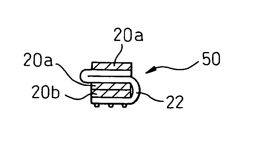
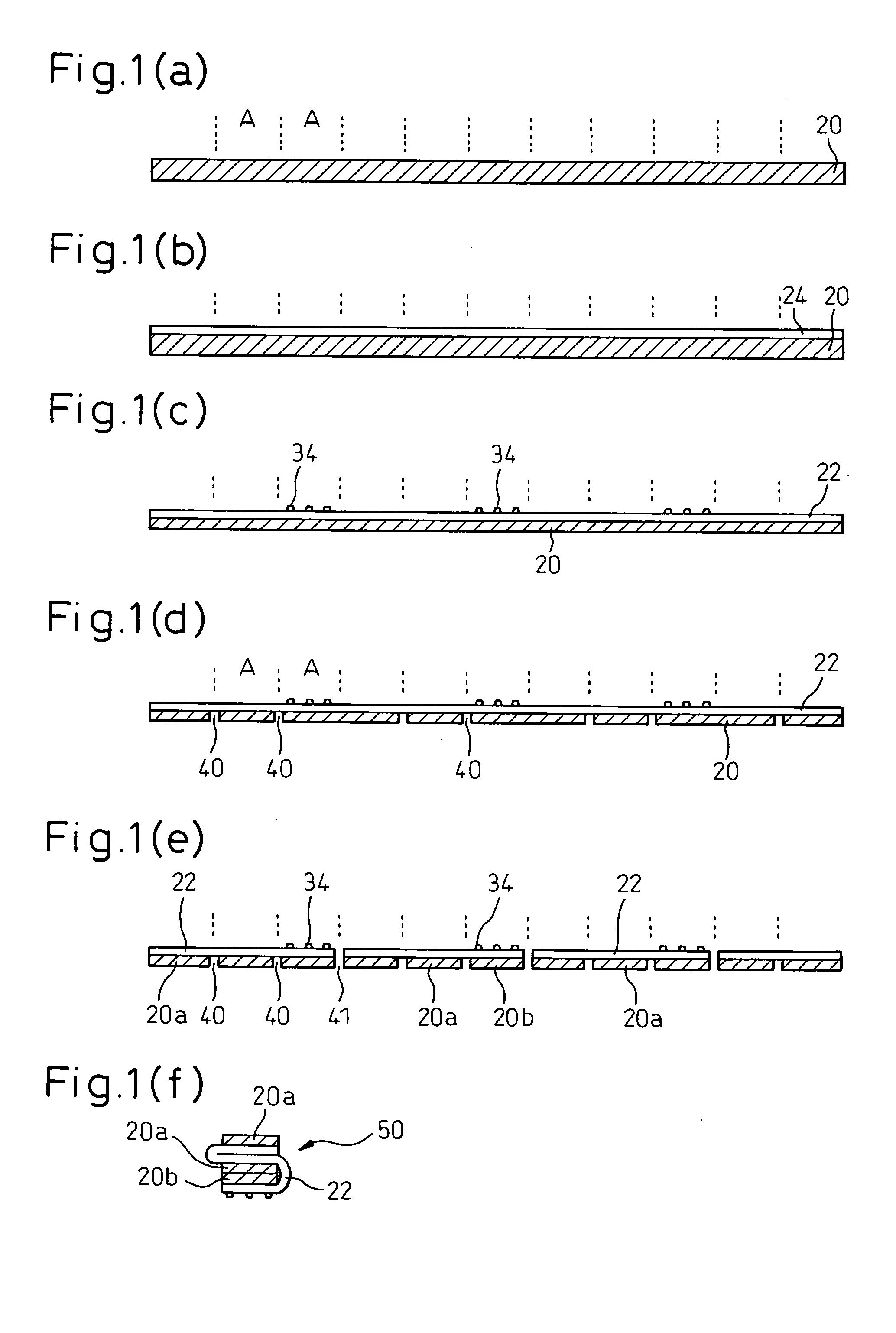
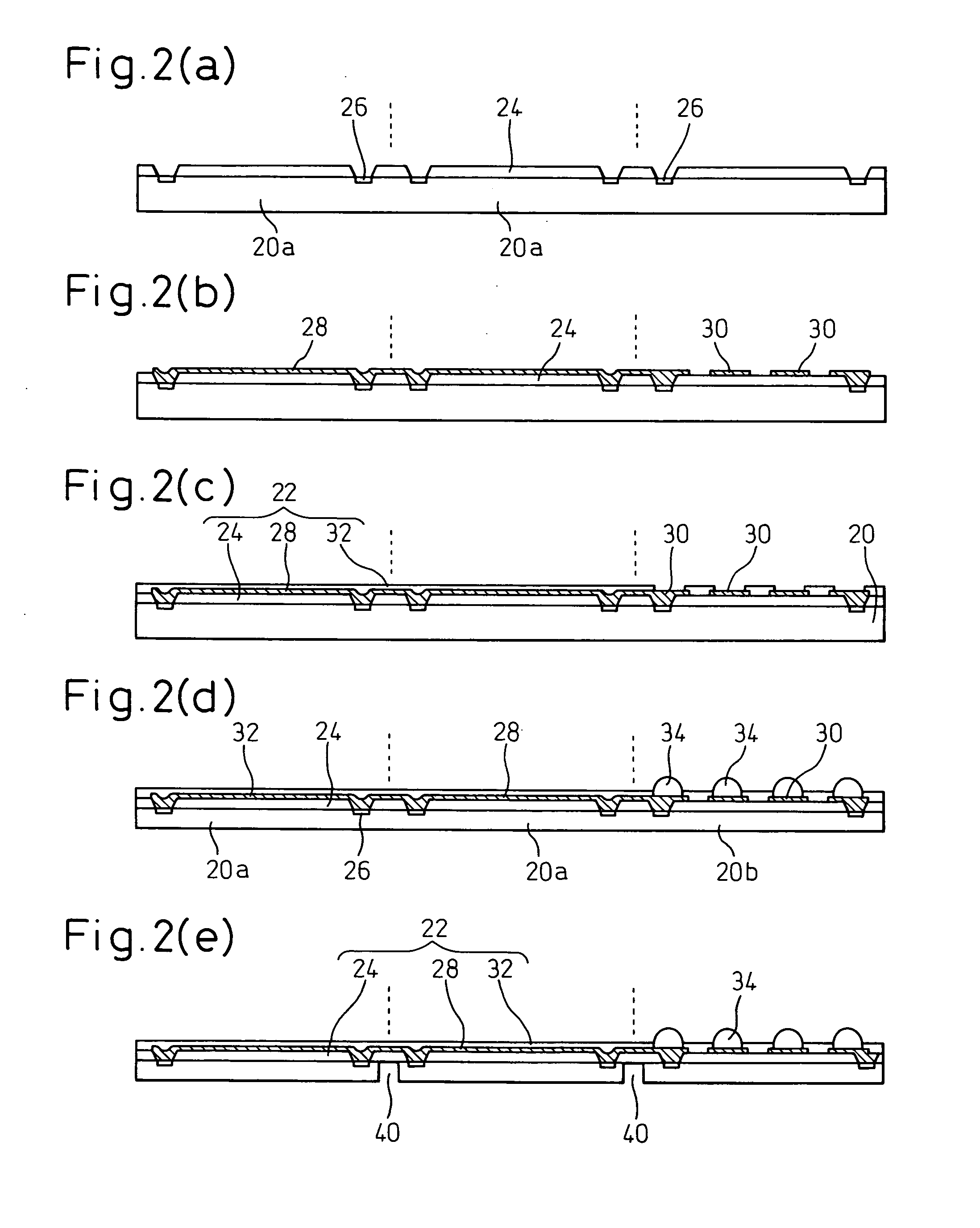
[0025] FIGS. 1(a) to 1(f) illustrate the inventive method for manufacturing a semiconductor device. According to the inventive method for manufacturing a semiconductor device, a semiconductor wafer carrying an insulating layer, a wiring pattern and external connection terminals on a surface thereof in a stage of a semiconductor wafer is divided into individual pieces so that a plurality of semiconductor elements constituting one semiconductor device are connected to each other by the insulating layer to form one piece, which is then folded to stack the semiconductor elements on each other. That is, the semiconductor device is characterized in that the semiconductor elements are stacked together in a so-called wafer stage.

[0026] In FIG. 1(a), a semiconductor wafer 20 is shown, in which semiconductor elements are arranged to form predetermined sections. In this regard, “A” denotes one section.

[0027] In FIG. 1(b), a surface of the semiconductor wafer 20, on which electrode terminals a...

second embodiment

[0046] In FIGS. 5(a) to 5(f), the inventive method for manufacturing a semiconductor device is illustrated. Also in this embodiment, in the similar manner as described with reference to the preceding embodiment, the re-wiring patterns are formed for electrically connecting the semiconductor elements in a wafer stage, and the flexible cover layer 22, covering the electrode terminal-forming surface of the semiconductor wafer 20, is folded to manufacture a semiconductor device in which a plurality of semiconductor elements are stacked together.

[0047] In FIG. 5(a), the semiconductor wafer 20 is illustrated. In FIG. 5(b), a characteristic manufacturing process in this embodiment is illustrated, in which the semiconductor wafer 20 is half-cut in the thickness direction in coincidence with the boundaries A of the semiconductor elements formed at a predetermined arrangement in the semiconductor wafer 20. Reference numeral 42 denotes a separation groove formed by half-cutting the semiconduct...


PUM


Abstract

A process for manufacturing a semiconductor device, the process comprising the steps of: covering an electrode terminal forming surface of a semiconductor wafer, on which a plurality of semiconductor elements are formed and arranged, with a cover layer comprising a flexible insulating film on which re-wiring patterns are formed, to adhere the cover layer to the electrode terminal forming surface, in such a manner that electrode terminals of the semiconductor elements are electrically connected with connecting terminals of the re-wiring patterns; forming the semiconductor wafer with grooves from the surface opposite to the electrode terminal forming surface thereof, so that the grooves extend along boundary lines of the semiconductor elements; dividing the semiconductor wafer with the cover layer to obtain a plurality of units, each unit comprising a plurality of the semiconductor elements and a sub-divided cover layer to define a single semiconductor device; and folding the cover layer of the respective divided unit along the grooves, so that at least some of the semiconductor elements in the respective unit are stacked.

Description

BACKGROUND OF THE INVENTION [0001] 1. Field of the Invention [0002] The present invention relates to a process for manufacturing a semiconductor device and, more specifically, it relates to a process for manufacturing a semiconductor device wherein semiconductor elements are laminated together in a stage of semiconductor wafers and capable to be mounted. [0003] 2. Description of the Related Art [0004] As shown in FIGS. 6(a) to 6(c), there is a product wherein semiconductor elements 12 (FIG. 6b) are carried on a flexible wiring board 10 (FIG. 6a) provided with external connection terminals 14 in a mounting area and the flexible wiring board 10 is folded as shown in FIG. 6c to stack the semiconductor elements 12 together (for example, in Japanese Unexamined Patent Publication (Kokai) Nos. 2000-307037, 2003-86760 and 2003-86761). Since a plurality of semiconductor elements can be mounted on one semiconductor device, the semiconductor device formed by stacking the semiconductor elements...

Claims


Application Information

Patent Timeline
IPC IPC(8): H01L25/18H01L21/301H01L21/56H01L21/68H01L21/78H01L21/98H01L23/525H01L23/538H01L25/065H01L25/07
CPCH01L21/6835H01L2224/73267H01L21/78H01L23/525H01L23/5387H01L25/0657H01L25/50H01L2221/68327H01L2221/68377H01L2225/06517H01L2225/06555H01L2225/06579H01L2924/30105H01L24/24H01L2224/24137H01L2224/32145H01L21/6836H01L2924/12042H01L2924/00
Inventor WATANABE, SHOJI
Owner SHINKO ELECTRIC IND CO LTD
Why Eureka
Try Eureka