Inspection apparatus
- Summary
- Abstract
- Description
- Claims
- Application Information
AI Technical Summary
Benefits of technology
Problems solved by technology
Method used
Image
Examples
first embodiment
[0070] [First Embodiment]
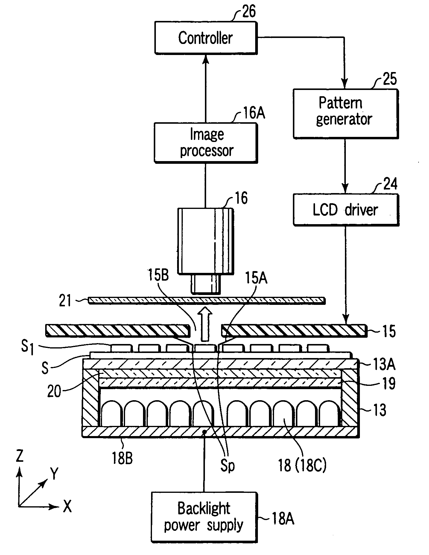
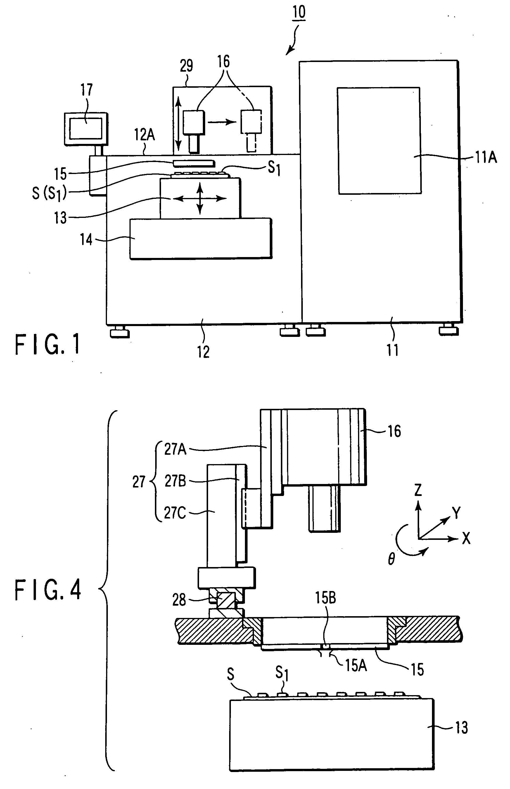
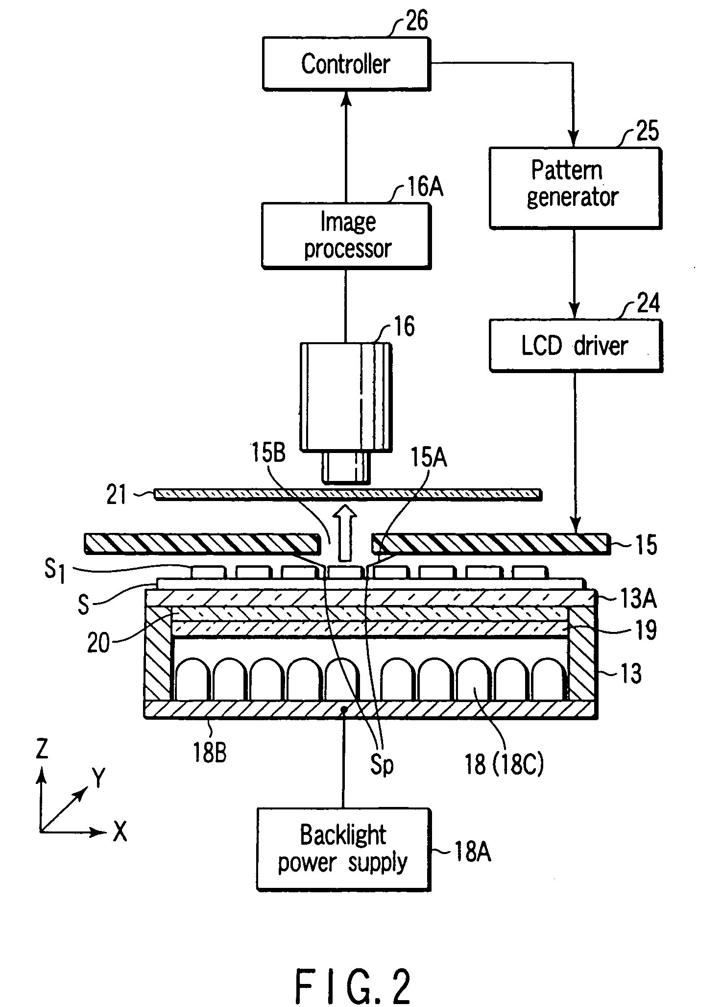
[0071] The inspection apparatus shown in FIG. 1 can be suitably used for, e.g., illuminated inspection for an LCD panel. This inspection apparatus 10 can include a loader chamber 11 which transports substrates (to be referred to as “LCD substrates” hereinafter) S on which LCD panels are formed, and a prober chamber 12 which is adjacent to the loader chamber 11 and in which illuminated inspection for the LCD substrates S is performed. The substrate can be a wafer-like substrate or a dicing-frame-like substrate. The LCD substrates S are transported from the loader chamber 11 into the prober chamber 12, and are subjected to illuminated inspection one by one in the prober chamber 12. Each LCD substrate S is a circular glass substrate with a diameter of 200 mm. Rectangular LCD panels S1 each with a side of approximately 20 mm can be arranged in a matrix on the upper surface of the LCD substrate S. Alternatively, one LCD panel S1 can be arranged on the LCD substra...
second embodiment
[0124] [Second Embodiment]
[0125]FIG. 9 is a view showing the main part of another embodiment of the present invention. This embodiment exemplifies an inspection apparatus suitably used for light-reception test for an image sensing element. The inspection apparatus according to this embodiment can include a loader chamber 11 for transporting a substrate (to be referred to as a “CCD substrate” hereinafter) on which a plurality of image sensing elements (e.g., CCD-type image sensing elements or MOS-type image sensing elements) S are formed, and a prober chamber 12 adjacent to the loader chamber to perform light-reception test for the CCD substrate. The loader chamber 11 can be formed in a manner similar to that of the LCD inspection apparatus shown in FIG. 1. Other than a wafer-type substrate, a dicing-type substrate can also be employed as the CCD substrate.
[0126] As shown in, e.g., FIG. 9, the prober chamber can include a stage 13, a probe card 15 arranged above the stage 13, and a ...
PUM
 Abstract
Description
Claims
Application Information


