AI technical title is built by Patsnap AI team. It summarizes the technical point description of the patent document.
a microchip and pre-molded technology, applied in the field of microchip packaging techniques, can solve the problems of affecting the operation of automobiles, affecting the quality of microchips, and affecting the accuracy of microchips, so as to reduce the moisture permeability and reduce the stress
Inactive Publication Date: 2005-02-17
ANALOG DEVICES INC
View PDF7 Cites 46 Cited by
Summary
Abstract
Description
Claims
Application Information
AI Technical Summary
This helps you quickly interpret patents by identifying the three key elements:
Problems solved by technology
Method used
Benefits of technology
Benefits of technology
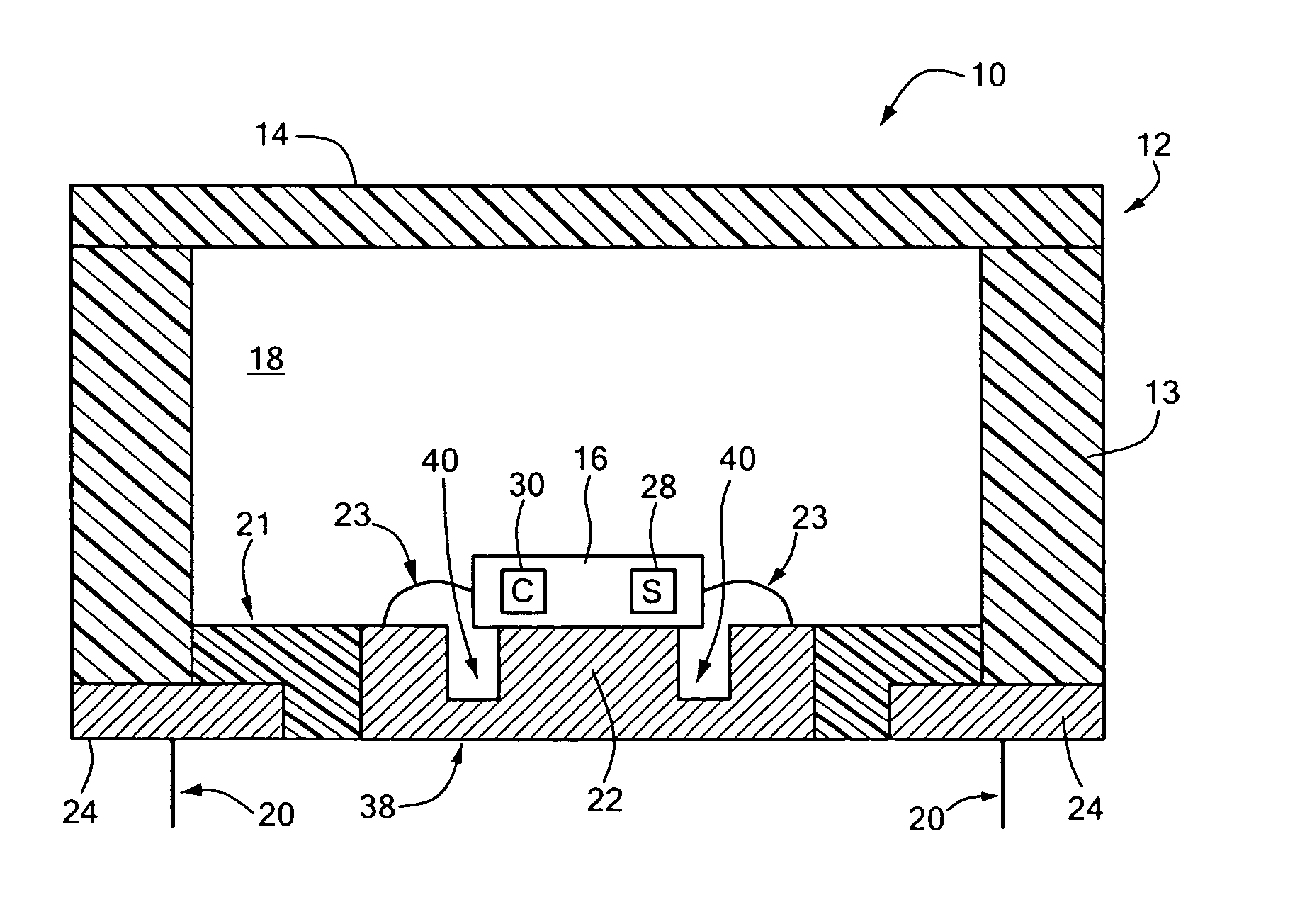
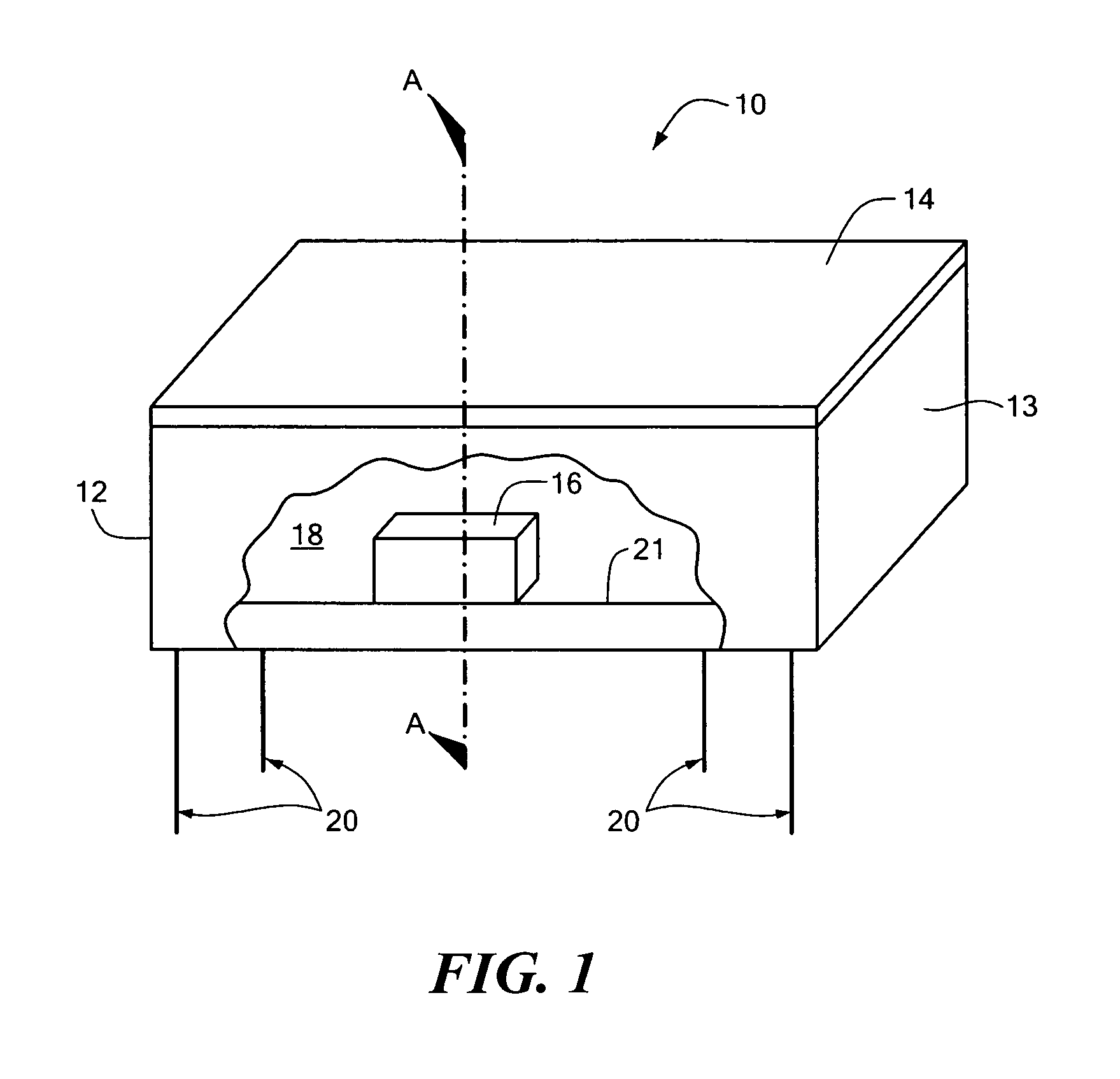
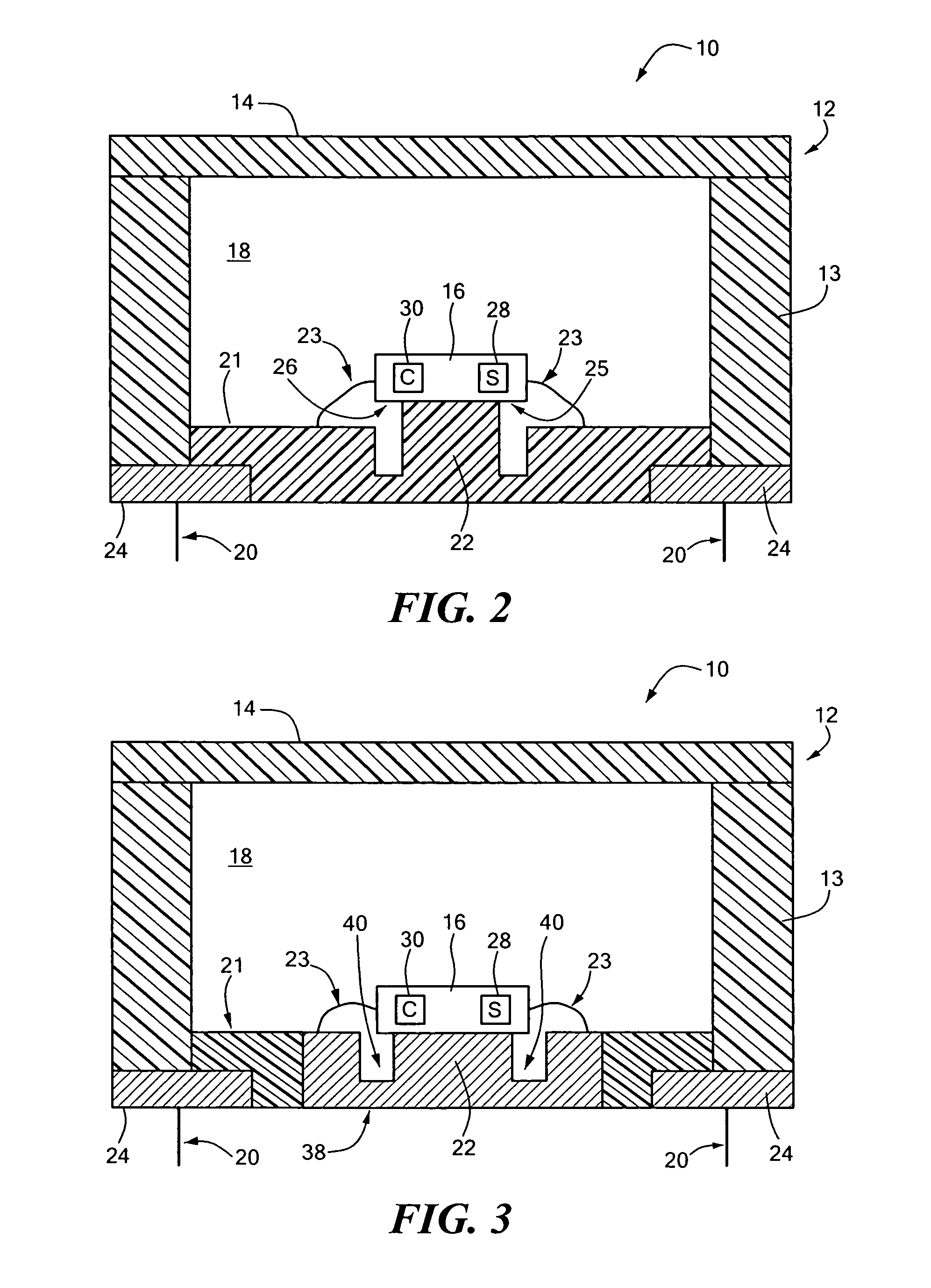
[0013] Different types of isolators may be used. For example, the isolator may be formed from the leadframe. Additionally or alternatively, the isolator may have a plurality of protrusions extending from the base of the cavity. In some embodiments, the isolator is formed from a low moisture permeability molding material. In still other embodiments, the isolator is at least in part formed from a silicone material. Such a soft moldable material should mitigate stresses. Other embodiments form the isolator, at least in part, from one or more different moldable materials.
Problems solved by technology
Specifically, this disparate expansion commonly is caused by mismatched coefficients of thermal expansion (“CTE”) between the materials forming the die bottom surface and the internal package surface that secures the die.
In fact, these CTE mismatches can cause the sensor to deliver incorrect motion measurements.
For example, when implemented as an accelerometer within an automobile airbag system or as a gyroscope in an automobile traction control system, CTE mismatches can produce results that can cause the automobile to operate erratically.
Consequently, such incorrect measurements can lead to bodily injury or death for drivers, their passengers, or others near the moving automobile (e.g., people in other automobiles).
Moreover, transfer molded and premolded packages also typically cannot provide hermeticity.
Undesirably, ceramic packages typically are more expensive than the other two types of packages.
In addition, securing a MEMS sensor die within a ceramic package requires a larger number of process steps (when compared to the other noted types of packages), thus further increasing production costs.
In fact, in many MEMS sensor applications using ceramic packages, the packaging cost far exceeds the cost of producing the MEMS sensor itself.
Method used
Image
Click on the blue label to locate the original text in one second.
Reading with bidirectional positioning of images and text.
Examples
Embodiment Construction
[0021] Illustrative embodiments of the invention substantially reduce chip stresses associated with conventional premolded-type packages so they can be successfully used to package stress sensitive microchips. Accordingly, because of the lower cost of premolded packages (when compared to ceramic packages), such embodiments can significantly reduce production costs while maintaining desired performance. Moreover, illustrative embodiments further enable premolded-type packages to provide hermetically sealed environments, thus enabling use with a variety of microchips requiring hermeticity. Details of illustrative embodiments are discussed below.
[0022]FIG. 1 schematically shows a partially cut-away isometric view of a packaged microchip 10 that can implement various embodiments of the invention. In illustrative embodiments, the packaged microchip 10 is a MEMS device implemented as an angular rate sensor. Accordingly, for illustrative purposes, various embodiments are discussed herein ...
PUM
Abstract
A MEMS inertial sensor is secured within a premolded-type package formed, at least in part, from a low moisture permeable molding material. Consequently, such a motion detector should be capable of being produced more economically than those using ceramic packages. To those ends, the package has at least one wall (having a low moisture permeability) extending from a leadframe to form a cavity, and an isolator (with a top surface) within the cavity. The MEMS inertial sensor has a movable structure suspended above a substrate having a bottom surface. The substrate bottom surface is secured to the isolator top surface at a contact area. In illustrative embodiments, the contact area is less than the surface area of the bottom surface of the substrate. Accordingly, the isolator forms a space between at least a portion of the bottom substrate surface and the package. This space thus is free of the isolator. Moreover, due to the low moisture permeability of the package, further production steps can be avoided while ensuring that moisture does not adversely affect the MEMS inertial sensor within the cavity.
Description
PRIORITY [0001] This patent application is a continuation-in-part of and claims the earliest priority date from U.S. patent application Ser. No. 10 / 369,776, filed Feb. 20, 2003, entitled, “PACKAGED MICROCHIP,” assigned attorney docket number 2550 / 162, and naming Lewis Long and Kieran Harney as inventors, the disclosure of which is incorporated herein, in its entirety, by reference. As a result of this priority claim, this patent application thus claims priority from parent U.S. patent application Ser. No. 10 / 234,215, filed Sep. 4, 2002, now U.S. Pat. No. 6,768,196, the disclosure of which is incorporated herein, in its entirety, by reference. [0002] This patent application also is a continuation-in-part of and claims priority from U.S. patent application Ser. No. 10 / 326,640, filed Dec. 19, 2002, entitled, “PACKAGED MICROCHIP WITH ISOLATOR HAVING SELECTED MODULUS OF ELASTICITY,” assigned attorney docket number 2550 / 163, and naming Maurice Karpman as inventor, the disclosure of which ...
Claims
Application Information
Patent Timeline
Application Date:The date an application was filed.
Publication Date:The date a patent or application was officially published.
First Publication Date:The earliest publication date of a patent with the same application number.
Issue Date:Publication date of the patent grant document.
PCT Entry Date:The Entry date of PCT National Phase.
Estimated Expiry Date:The statutory expiry date of a patent right according to the Patent Law, and it is the longest term of protection that the patent right can achieve without the termination of the patent right due to other reasons(Term extension factor has been taken into account ).
Invalid Date:Actual expiry date is based on effective date or publication date of legal transaction data of invalid patent.
Patent Type & AuthorityApplications(United States)

