Memory controller that selectively changes frequency of a memory clock signal, a smart card including the same, and a method of controlling a read operation of a memory

a memory clock signal and memory controller technology, applied in the field of memory devices, can solve problems such as system performance degradation, and achieve the effects of improving system performance, preventing memory, and improving system performan

Active Publication Date: 2005-02-17
SAMSUNG ELECTRONICS CO LTD
View PDF5 Cites 14 Cited by
  • Summary
  • Abstract
  • Description
  • Claims
  • Application Information

AI Technical Summary

Benefits of technology

[0015] The present invention provides a memory controller that prevents a memory from outputting erroneous data when operating at a high frequency and improves the performance of a system in which a read operation of the memory is frequently executed. In addition, the present invention provides a smart card including a memory controller that prevents a memory from outputting erroneous data when operating at a high frequency and improves the performance of a system in which a read operation of the memory is frequently executed. Further, the present invention provides a method of controlling a read operation of a memory using a memory controller that prevents the memory from outputting erroneous data when operating at a high frequency and improves the operation performance of a system in which a read operation of the memory is frequently executed.

Problems solved by technology

In a system in which the read operation of the memory 20 is frequently executed, however, the performance of the system deteriorates as the frequency of the memory clock signal MCLK decreases.

Method used


Image

  • Memory controller that selectively changes frequency of a memory clock signal, a smart card including the same, and a method of controlling a read operation of a memory
  • Memory controller that selectively changes frequency of a memory clock signal, a smart card including the same, and a method of controlling a read operation of a memory
  • Memory controller that selectively changes frequency of a memory clock signal, a smart card including the same, and a method of controlling a read operation of a memory

Examples


Embodiment Construction

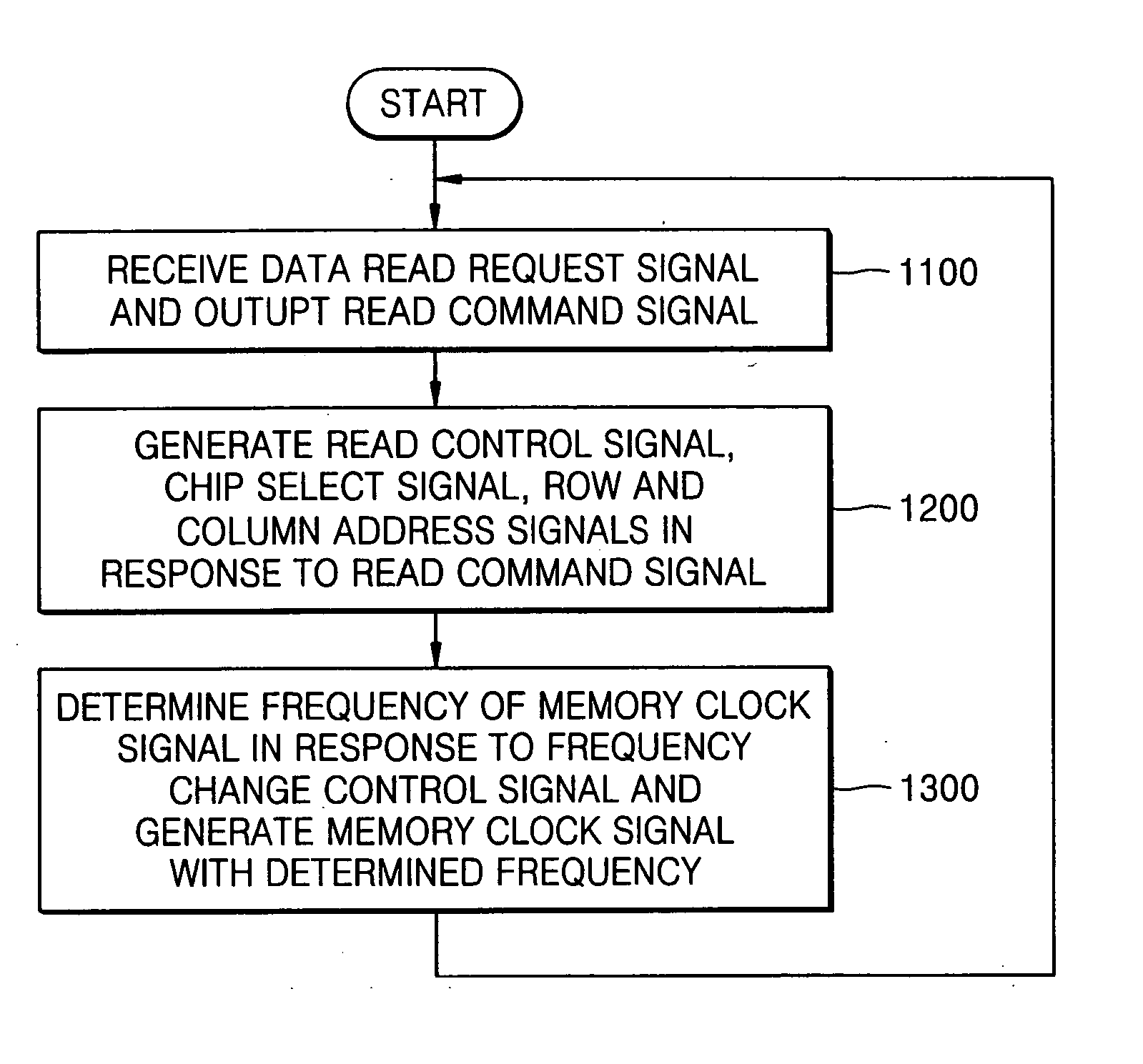
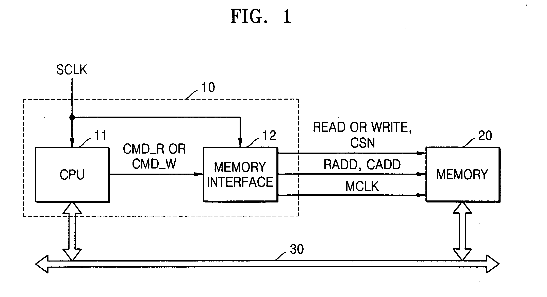
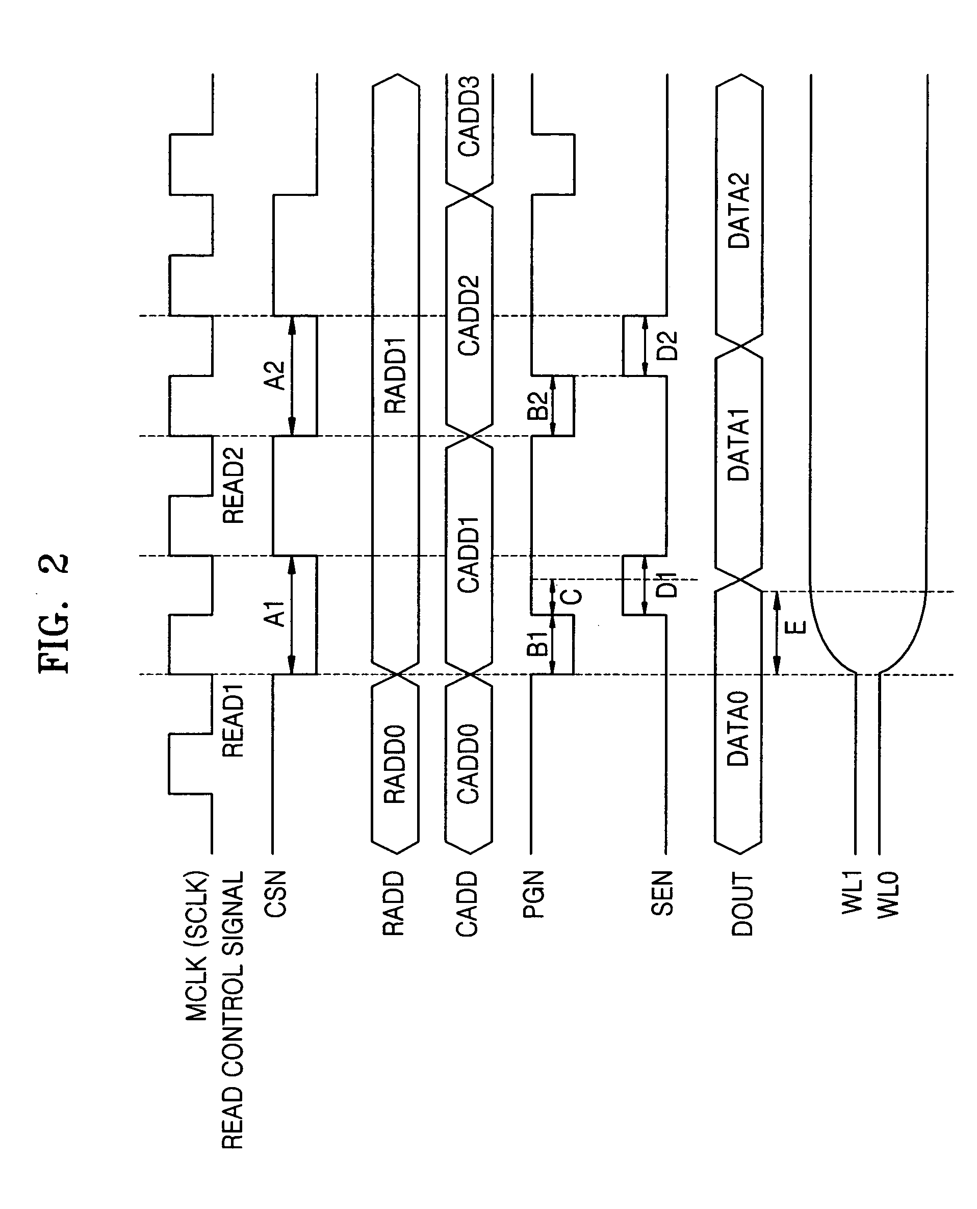
[0030]FIG. 4 is a block diagram of a memory controller 110 and a memory 120 according to an exemplary embodiment of the present invention. Referring to FIG. 4, the memory controller 110 includes a central processing unit (CPU) 111, a memory interface 112, and a frequency change controller 113. The memory interface 112 is connected to the memory 120. The CPU 111 outputs a read command signal CMD_R or a write command signal CMD_W to the memory interface 112 when the CPU 111 receives an external data read request signal DRQ or an external data write request signal DWQ.

[0031] The memory interface 112 outputs a data read control signal READ or a data write control signal WRITE to the memory 120 in response to the read command signal CMD_R or write command signal CMD_W, respectively. In addition, the memory interface 112 outputs a chip select signal CSN, a row address signal RADD and a column address signal CADD to the memory 120. While FIG. 4 illustrates the memory interface 112 outputt...


PUM


Abstract

Provided are a memory controller that selectively changes a frequency of a memory clock signal, a smart card including the memory controller, and a method of controlling a read operation of a memory. The memory controller includes a central processing unit (CPU), a memory interface, and a frequency change controller. The CPU outputs a read command signal in response to a data read request signal and outputs a write command signal in response to a data write request signal. The memory interface outputs a plurality of control signals in response to one of the read command signal and the write command signal, generates a memory clock signal based on a system clock signal, and changes a frequency of the memory clock signal in response to a frequency change control signal. The frequency change controller outputs the frequency change control signal in response to the plurality of control signals and the memory clock signal. The memory controller, the smart card including the memory controller, and the method of controlling a read operation of a memory prevent the memory from outputting erroneous data when the memory is operated at a high frequency.

Description

CROSS-REFERENCE TO RELATED APPLICATION [0001] This application claims priority to Korean Patent Application No. 2003-55876, filed on Aug. 12, 2003, in the Korean Intellectual Property Office, the disclosure of which is incorporated herein in its entirety by reference. BACKGROUND OF THE INVENTION [0002] 1. Technical Field [0003] The present invention relates to a memory device, and more particularly, to a method of controlling a read operation of a memory device. [0004] 2. Discussion of the Related Art [0005] With the development of semiconductor manufacturing technology, a system-on-chip (SOC), in which a plurality of system chips are integrated into a single chip, has been proposed. The SOC typically includes a memory that stores an operating system (OS) program or data that is generated when the OS program is executed. [0006] In general, a memory includes a memory cell array having a matrix structure. The memory receives a row address signal, a column address signal, and a data re...

Claims


Application Information

Patent Timeline
Patent Type & Authority Applications(United States)
IPC IPC(8): G06F12/00G06K19/07G06K7/00G11C7/00G11C7/22
CPCG06K7/0008G11C7/222G11C7/22G11C7/00
Inventor KIM, MIN-KYU
Owner SAMSUNG ELECTRONICS CO LTD
Why Eureka
Try Eureka