Method of operating a memory system including an integrated circuit buffer device

a memory system and buffer device technology, applied in the field of memory systems, memory subsystems, memory modules or systems having memory devices, can solve the problems of reducing signaling performance, limiting system operating frequency, and requiring high throughput for bandwidth intensive applications, so as to eliminate physical interdependence

Inactive Publication Date: 2005-02-24
RAMBUS INC
View PDF99 Cites 91 Cited by
  • Summary
  • Abstract
  • Description
  • Claims
  • Application Information

AI Technical Summary

Benefits of technology

[0016] The present invention is directed toward memory system architectures (i.e., interconnect topologies) which include a controller communicating to at least one memory subsystem (e.g., a buffered memory module). An independent point-to-point link may be utilized between the controller and each memory subsystem to eliminate physical inter-dependence between memory subsystems. According to an embodiment, the memory system may be upgraded by coupling additional memory module(s), each via a dedicated point-to-point link to the controller. Bandwidth may scale upwards as the memory system is upgraded by the additional memory module(s).

Problems solved by technology

In addition to upgradeability, many of these contemporary memory systems also require high throughput for bandwidth intensive applications, such as graphics.
Impedance discontinuities may produce undesirable voltage reflections manifested as signal noise that may ultimately limit system operating frequency.
The load capacitances connected to multiple points along the length of the signal line may degrade signaling performance.
In addition, impedance along the signal line may become harder to control or match as more load capacitances are present along the signal line.
Mismatched impedance may introduce voltage reflections that cause signal detection errors.
As memory systems incorporate an increasing number of memory module configurations, the verification and validation of the number of permutations that these systems make possible may become increasingly more time consuming.
More time required to test a system often increases the cost of bringing the system to market or delays a product introduction beyond an acceptable window of time to achieve competitiveness.
However, the bussed approach may suffer from bandwidth limitations that stem from the electrical characteristics inherent in the bus topology.
In addition, impedance along a signal line may be increasingly more difficult to control with increased connection points along a signal line, introducing impedance mismatch and signal reflections.

Method used


Image

  • Method of operating a memory system including an integrated circuit buffer device
  • Method of operating a memory system including an integrated circuit buffer device
  • Method of operating a memory system including an integrated circuit buffer device

Examples


Embodiment Construction

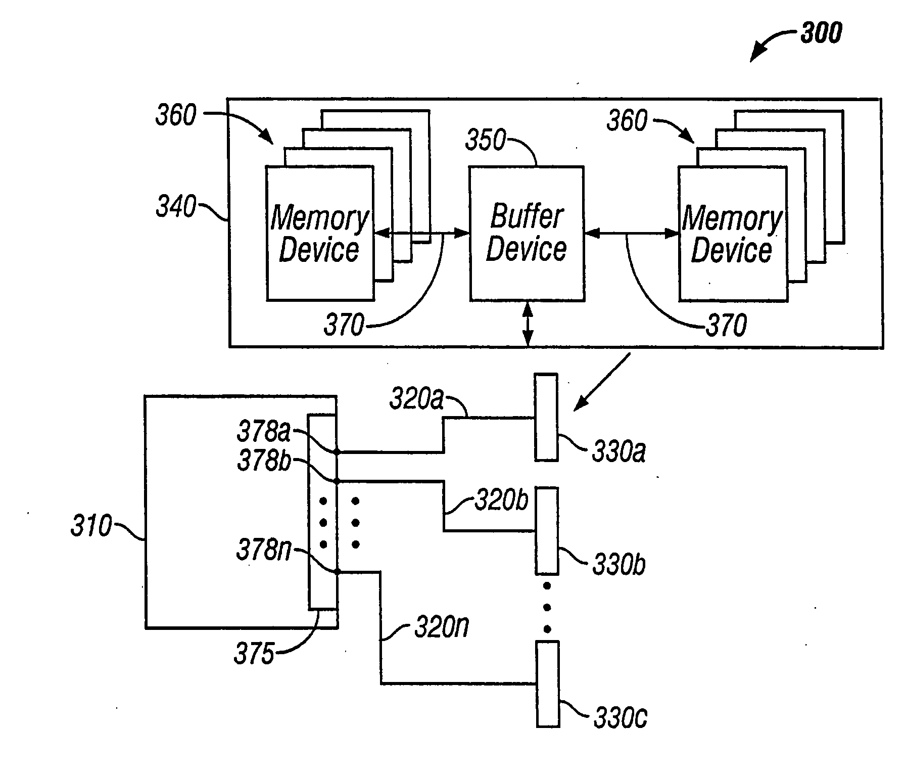
[0032] The present invention relates to a memory system which includes a plurality of point-to-point links connected to a master. At least one point-to-point link connects at least one memory subsystem to the master, (e.g., a processor or controller). The memory system may be upgraded by coupling memory subsystems to the master via respective dedicated point-to-point links. Each memory subsystem includes a buffer device that communicates to a plurality of memory devices. The master communicates with each buffer device via each point-to-point link. The buffer device may be disposed on a memory module along with the plurality of memory devices and connected to the point-to-point link via a connector. Alternatively, the buffer device may be disposed on a common printed circuit board or backplane link along with the corresponding point-to-point link and master.

[0033]“Memory devices” are a common class of integrated circuit devices that have an array of memory cells, such as, dynamic ra...


PUM


Abstract

A memory system architecture / interconnect topology that includes at least one point-to-point link between a master, and at least one memory subsystem. The memory subsystem includes a buffer device coupled to a plurality of memory devices. The memory system may be upgraded through dedicated point-to-point links and corresponding memory subsystems. The master communicates to the plurality of memory devices in each memory subsystem through the respective buffer device via each point-to-point link

Description

BACKGROUND OF THE INVENTION [0001] This invention relates to memory systems, memory subsystems, memory modules or a system having memory devices. More specifically, this invention is directed toward memory system architectures which may include integrated circuit devices such as one or more controllers and a plurality of memory devices. [0002] Some contemporary memory system architectures may demonstrate tradeoffs between cost, performance and the ability to upgrade, for example; the total memory capacity of the system. Memory capacity is commonly upgraded via memory modules or cards featuring a connector / socket interface. Often these memory modules are connected to a bus disposed on a backplane to utilize system resources efficiently. System resources include integrated circuit die area, package pins, signal line traces, connectors, backplane board area, just to name a few. In addition to upgradeability, many of these contemporary memory systems also require high throughput for ban...

Claims


Application Information

Patent Timeline
IPC IPC(8): G06F12/00G06F13/16G11C5/00G11C7/10G11C29/02
CPCG06F13/1673G06F13/1684G11C5/04G11C29/50012G11C29/02G11C29/028G11C7/10
Inventor PEREGO, RICHARD E.SIDIROPOULOS, STEFANOSTSERN, ELY
Owner RAMBUS INC
Why Eureka
Try Eureka