Method of manufacturing integrated circuit device including recessed channel transistor

a manufacturing method and integrated circuit technology, applied in the direction of semiconductor devices, basic electric elements, electrical equipment, etc., can solve the problems of new technical problems to be solved, shortening the channel length of transistors, and malfunctioning of integrated circuit devices

Inactive Publication Date: 2005-02-24
SAMSUNG ELECTRONICS CO LTD
View PDF3 Cites 104 Cited by
  • Summary
  • Abstract
  • Description
  • Claims
  • Application Information

AI Technical Summary

Benefits of technology

[0012] Some embodiments of the invention provide a method of manufacturing an integrated circuit device including a recessed channel transistor in which a gate trench with a planarized bottom is formed by preventing the formation of a silicon fence. Other embodiments provide a method of manufacturing an integrated circuit device including a recessed channel transistor in which a defect on an upper edge of an active region is prevented.

Problems solved by technology

As the integration density of integrated circuit devices increases, new technical problems to be solved emerge.
One of these problems is that the channel lengths of transistors are becoming shorter.
The SCE causes a punch through problem between a source and a drain resulting in a malfunction of the integrated circuit device, thereby reducing reliability of the integrated circuit.
When there is an especially short channel region in the recessed channel transistor, the threshold voltage of the transistor is not only reduced but a malfunction of the integrated circuit device results from a sub-threshold leakage current through the region.

Method used


Image

  • Method of manufacturing integrated circuit device including recessed channel transistor
  • Method of manufacturing integrated circuit device including recessed channel transistor
  • Method of manufacturing integrated circuit device including recessed channel transistor

Examples


Embodiment Construction

[0020] Hereinafter, the invention will be described more fully with reference to the accompanying drawings in which exemplary embodiments of the invention are shown. This invention may be, however, be embodied in many different forms and should not be construed as being limited to the embodiments set forth herein. Rather, these embodiments are provided so that this disclosure is thorough and complete and fully conveys the concept of the invention to those skilled in the art. In the drawings, the thicknesses of films or regions may be exaggerated for clarity. Like reference numerals refer to like elements throughout the drawings.

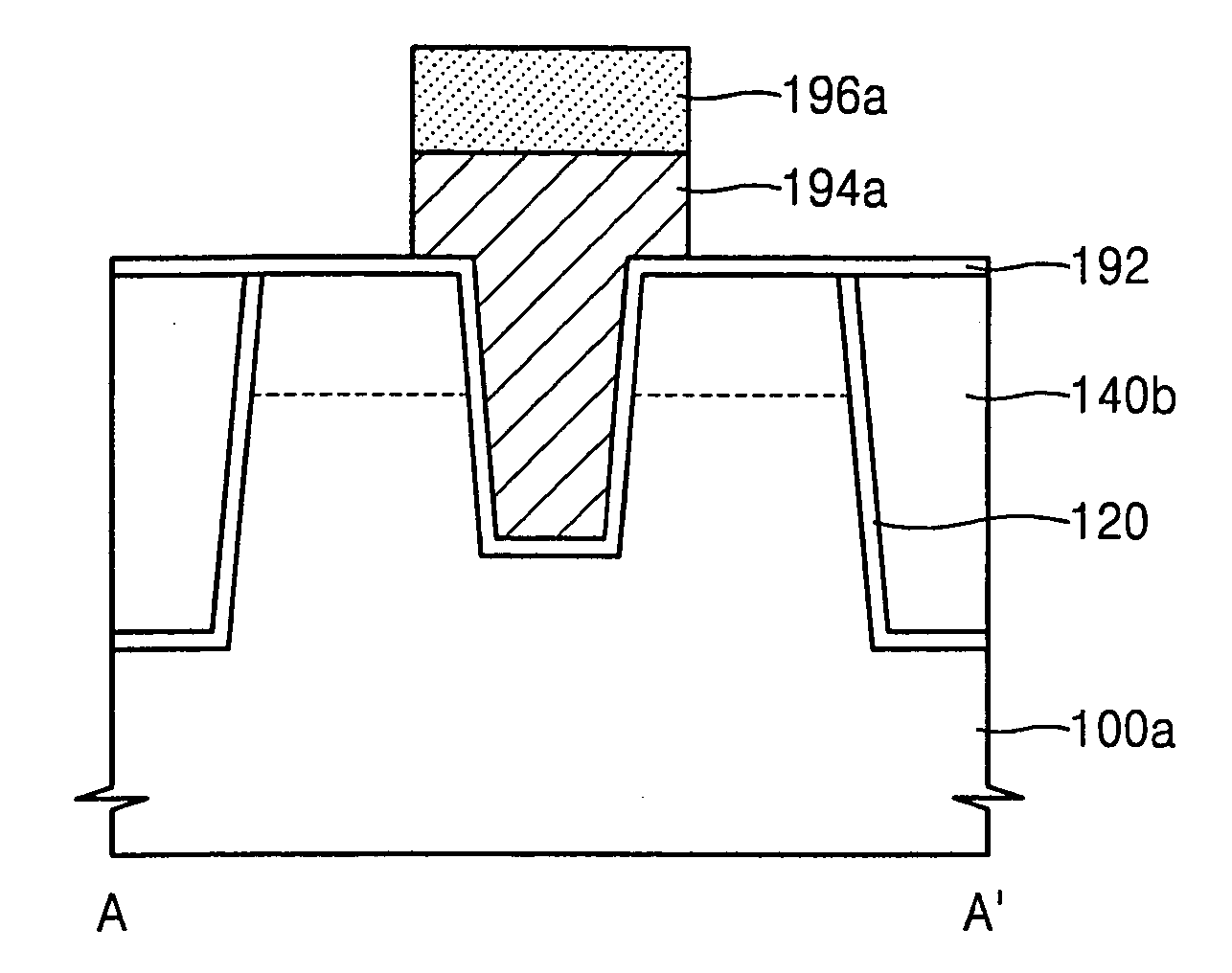
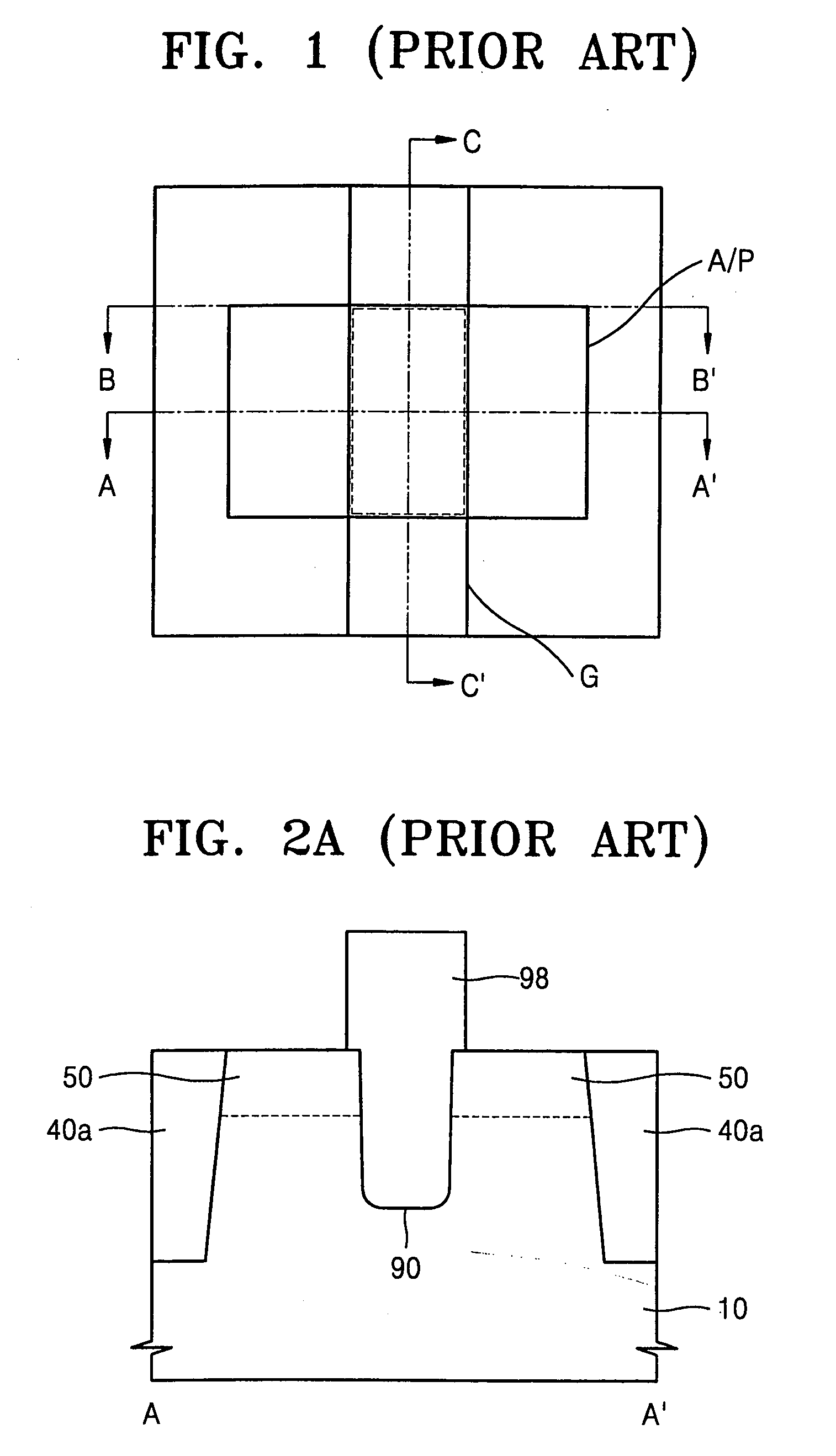
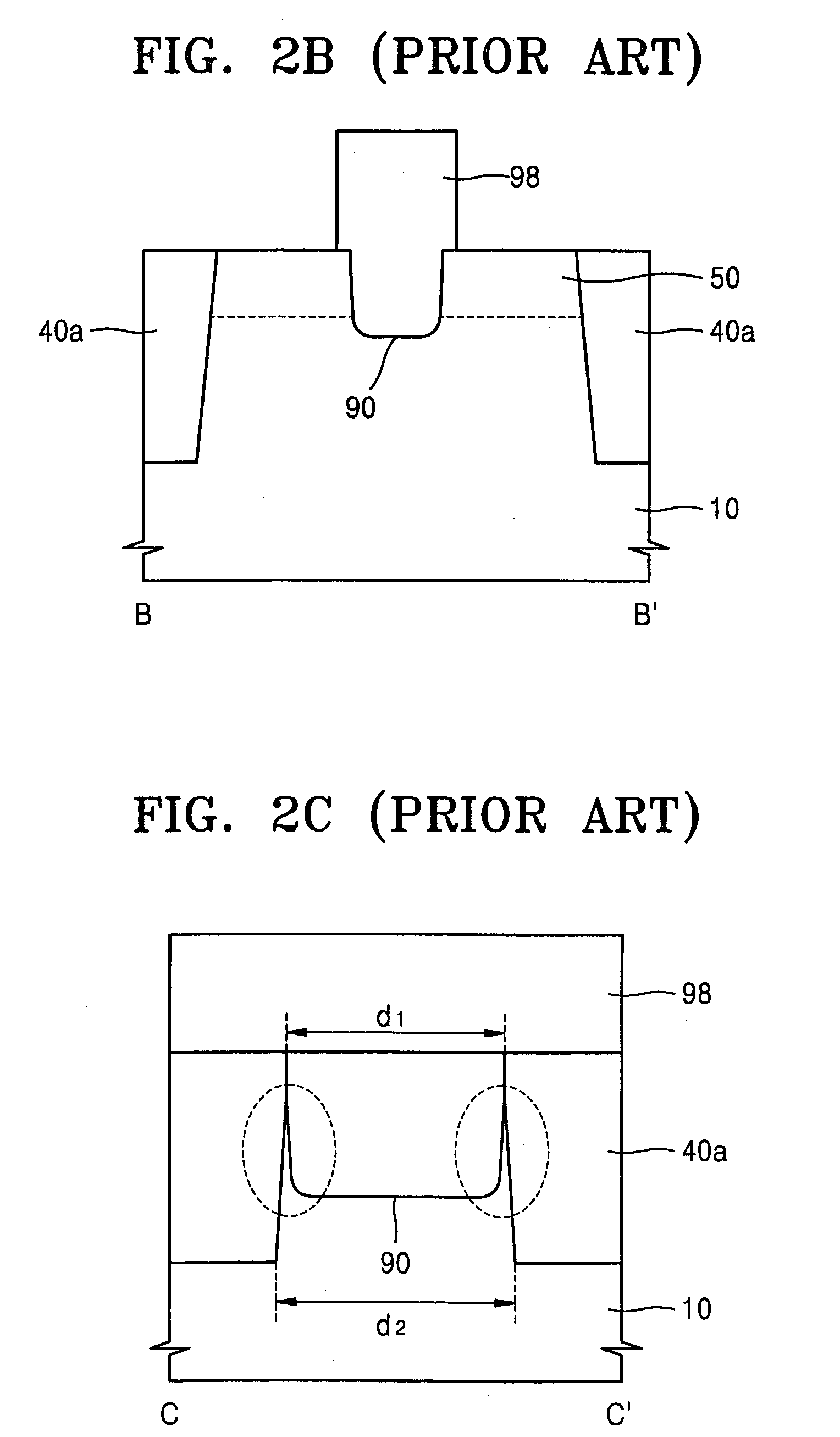
[0021]FIGS. 3A and 3B through 14A and 14B are cross-sectional diagrams illustrating a method of manufacturing a recessed transistor of an integrated circuit device according to some embodiments of the invention. FIGS. 3A, 4A, . . . 13A, and 14A are cross-sectional diagrams taken along the line A-A′. FIGS. 3B, 4B, . . . 13B, and 14B are cross-sectional diagra...


PUM


Abstract

A method according to some embodiments of the invention includes defining an active region by forming a trench device isolation region on an integrated substrate, forming a mask pattern that exposes a channel sub-region of the active region and the trench device isolation region adjacent to the channel sub-region, etching the trench device isolation region, which is exposed by the mask pattern, to be recessed to a first depth using the mask pattern as an etch mask, etching the channel sub-region to form a gate trench having a second depth that is deeper than the first depth using the mask pattern as an etch mask, and forming a recess gate that fills the gate trench.

Description

CROSS REFERENCE TO RELATED APPLICATIONS [0001] This application claims priority from Korean Patent Application No. 2003-57506, filed on 20 Aug. 2003, and from Korean Patent Application No. 2003-92585, filed on 17 Dec. 2003, the disclosures of which are incorporated by reference in their entirety for all purposes. BACKGROUND OF THE INVENTION [0002] 1. Field of the Invention [0003] This disclosure relates to a method of manufacturing an integrated circuit device, and more particularly, to a method of manufacturing an integrated circuit device that includes a recessed channel transistor. [0004] 2. Description of the Related Art [0005] As the integration density of integrated circuit devices increases, new technical problems to be solved emerge. One of these problems is that the channel lengths of transistors are becoming shorter. In the case of a planarized transistor, a channel length of the transistor is reduced as the integration density increases often resulting in a short channel ...

Claims


Application Information

Patent Timeline
Patent Type & Authority Applications(United States)
IPC IPC(8): H01L21/336H01L21/4763H01L29/78
CPCH01L29/66553H01L29/7834H01L29/66621
Inventor PARK, JONG-CHULSEO, JUNAHN, TAE-HYUKKWON, HYUK-JINSONG, JONG-HEUIKANG, DAE-KEUN
Owner SAMSUNG ELECTRONICS CO LTD
Why Eureka
Try Eureka