
Method of clock driven cell placement and clock tree synthesis for integrated circuit design

a technology of integrated circuit design and clock driven cell, which is applied in the field of design and manufacture of integrated circuits, can solve problems such as the reduction of the maximum operating frequency performance capability

Active Publication Date: 2005-03-03
BELL SEMICON LLC
View PDF11 Cites 45 Cited by
  • Summary
  • Abstract
  • Description
  • Claims
  • Application Information

AI Technical Summary

Benefits of technology

[0012] (d) performing a cell placement to minimize a function of propagation delay and maximum distance between flip-flops within each timing group; and

Problems solved by technology

Both clock skew and clock jitter may result in decreased performance capability in terms of maximum operating frequency and in circuit malfunction from setup and hold time violations.

Method used


Image

  • Method of clock driven cell placement and clock tree synthesis for integrated circuit design
  • Method of clock driven cell placement and clock tree synthesis for integrated circuit design
  • Method of clock driven cell placement and clock tree synthesis for integrated circuit design

Examples


Embodiment Construction

[0033] A disadvantage of previous methods of distributing a clock signal in an integrated circuit design is that they do not take into account the timing constraints in the data paths between flip-flops that are clocked by a common clock signal. Timing violations that result from the clock distribution design require an iterative process of redesign and optimization of the clock distribution network, which may significantly increase the design time and cost of the integrated circuit design.

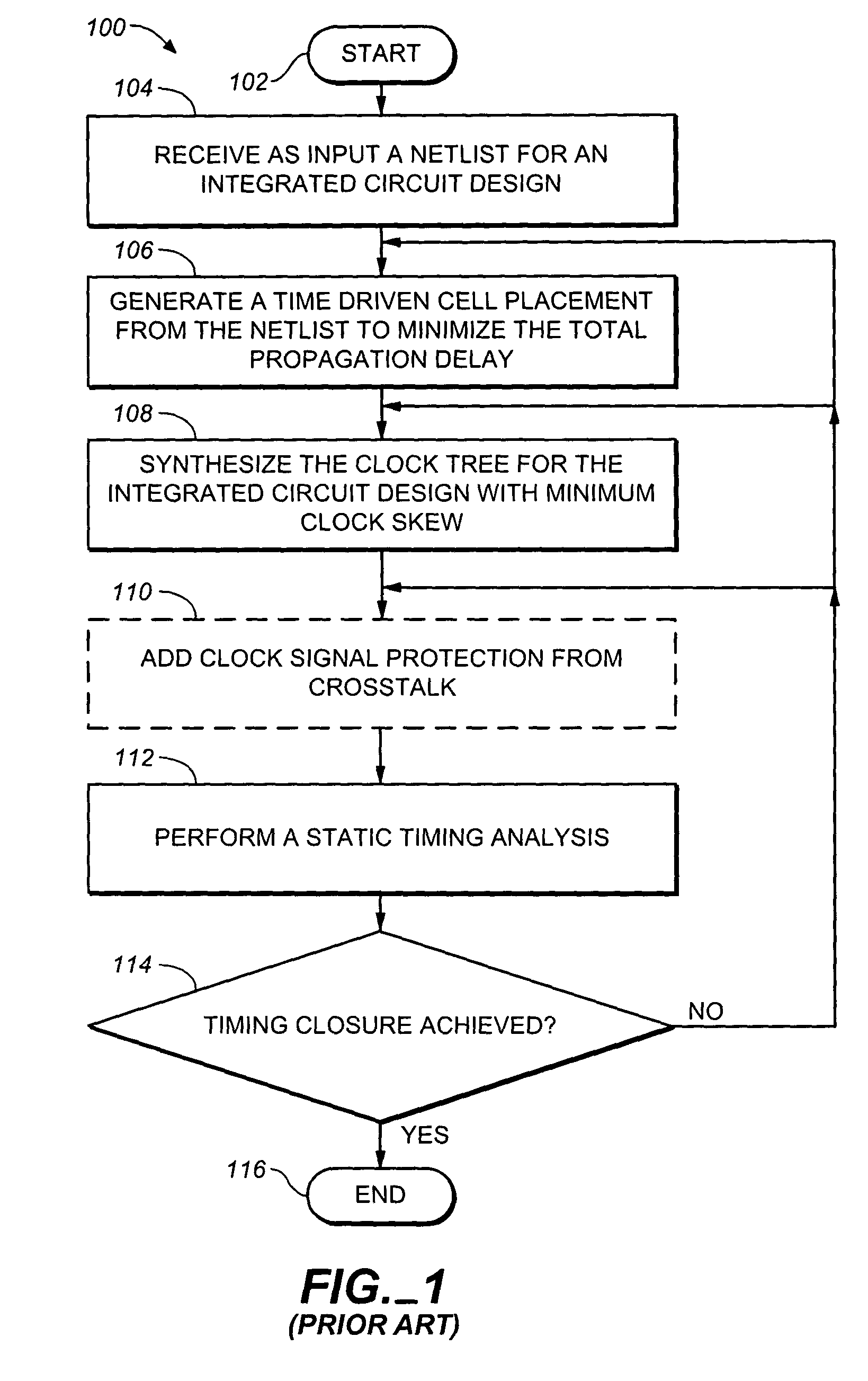
[0034]FIG. 1 illustrates a flow chart of a design flow of the prior art for an integrated circuit design.

[0035] Step 102 is the entry point of the flow chart 100.

[0036] In step 104, a netlist of an integrated circuit design is received as input. The netlist includes information as to what cells are to be placed and how they are connected to one another.

[0037] In step 106, a time driven cell placement is generated from the netlist that typically minimizes the total propagation delay.

[0038] In ...


PUM


Abstract

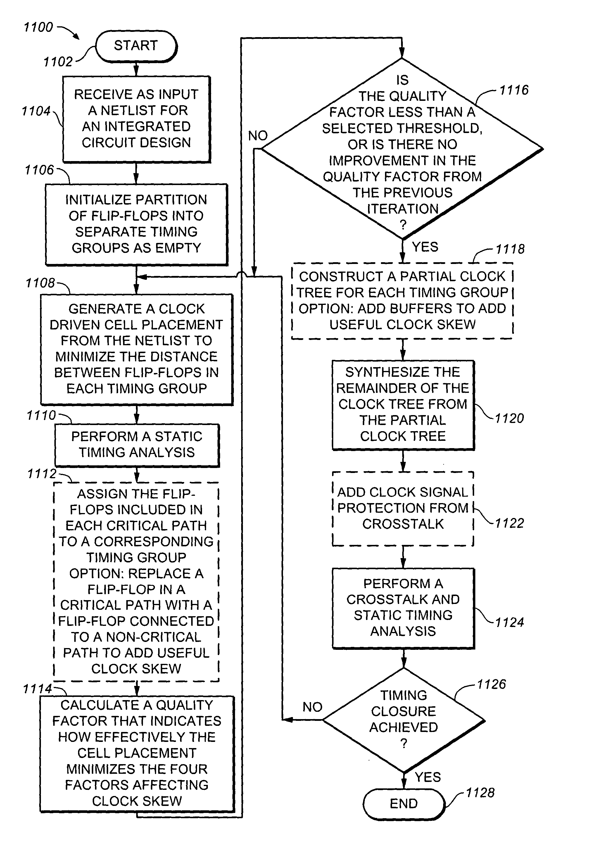
A method of cell placement and clock tree synthesis includes steps of: (a) identifying critical paths in an integrated circuit design; (b) partitioning the integrated circuit design into a timing group for each of the critical paths; (c) assigning each flip-flop in a critical path to a timing group corresponding to the critical path; (d) performing a cell placement to minimize a function of propagation delay and maximum distance between flip-flops within each timing group; and (e) constructing a clock sub-net for each timing group.

Description

BACKGROUND OF THE INVENTION [0001] 1. Field of the Invention [0002] The present invention relates generally to the design and manufacture of integrated circuits. More specifically, but without limitation thereto, the present invention relates to methods of distributing a common clock signal for an integrated circuit design within timing constraints that are determined by the selection and arrangement of clocked logic elements in the circuit design. [0003] 2. Description of Related Art [0004] Clock signals are widely used in integrated circuit designs to coordinate generation and propagation of logic functions across an integrated circuit die. The distribution of a clock signal to various locations across the integrated circuit die is an important aspect of the circuit design. The difference in the arrival time of a common clock signal at various locations in the physical layout of an integrated circuit design, or floorplan, is called clock skew. The variation in the clock period at ...

Claims


Application Information

Patent Timeline
Patent Type & Authority Applications(United States)
IPC IPC(8): G06F9/45G06F17/50
CPCG06F2217/62G06F17/5072G06F30/392G06F30/396
Inventor TETELBAUM, ALEXANDER
Owner BELL SEMICON LLC
Learn More