Fault isolation of circuit defects using comparative magnetic field imaging

a technology of comparative magnetic field imaging and fault isolation, applied in the direction of instruments, electrographic processes, material magnetic variables, etc., can solve the problems of cracking signal traces, affecting the localization of circuit defects, and increasing the impedance of signal lines to beyond the designed specification

Active Publication Date: 2005-03-17
NEOCERA
View PDF5 Cites 27 Cited by
  • Summary
  • Abstract
  • Description
  • Claims
  • Application Information

AI Technical Summary

Problems solved by technology

As integrated circuitry becomes increasingly compact and the packaging associated therewith becomes more complex, the localization of circuit defects becomes correspondingly difficult.
The localization of flaws is particularly difficult for those classified to the high resistance (HR) defect class of packaging and interconnect anomalies causing an increase in the impedance of a signal line to beyond the designed specification thereof.
These HR defects include cracked signal traces, cracked plated through-holes, delaminated vias and improperly wetted controlled collapse chip connection (C4) bumps.
Such HR defects can result in devices that do not operate at optimum speed, have an increased

Method used


Image

  • Fault isolation of circuit defects using comparative magnetic field imaging
  • Fault isolation of circuit defects using comparative magnetic field imaging
  • Fault isolation of circuit defects using comparative magnetic field imaging

Examples


Embodiment Construction

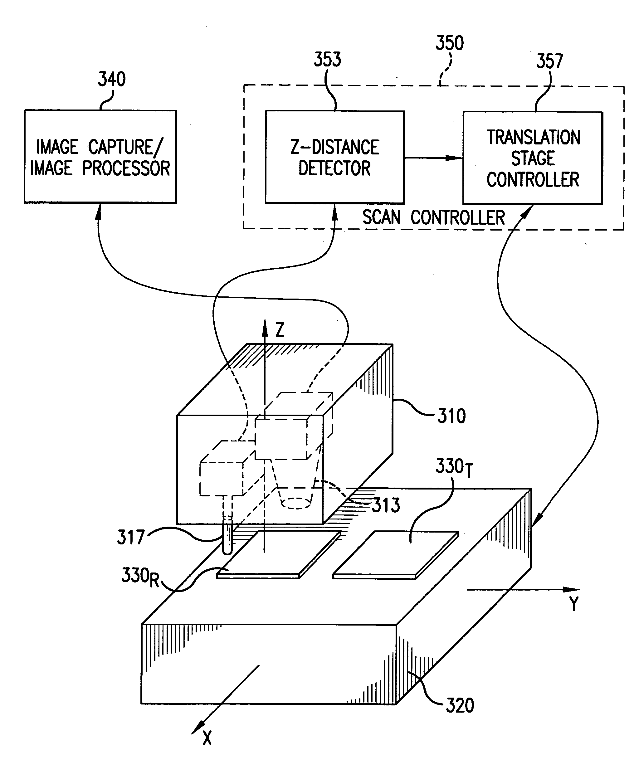
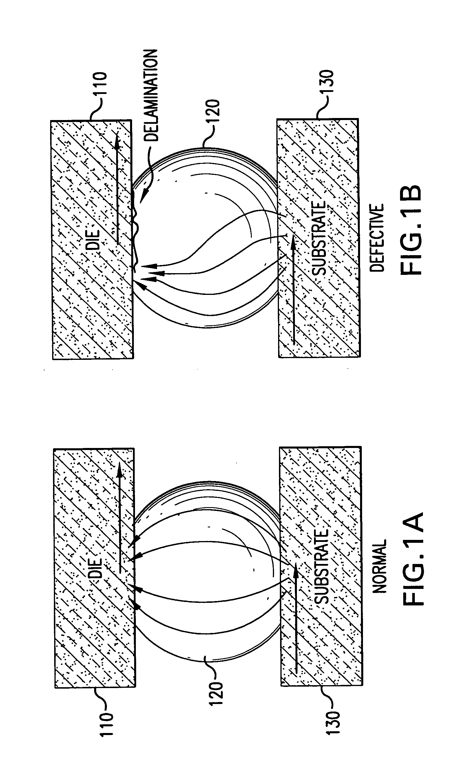
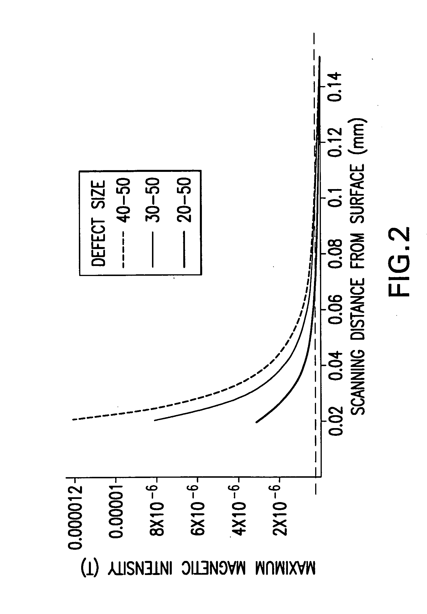
The method of the present invention constitutes a novel approach to isolating circuit defects, such as high resistance (HR) defects, using current imaging and comparative image analysis. Current imaging is based on the measurement and spatial mapping of the magnetic field generated by current carried in the structures of a device-under-test (DUT). Comparative image analysis identifies local differences between images. By way of the precise current imaging and subsequent comparative image analysis, the present invention attains localization of circuit defects to within tens of microns.

As is well known, the characteristic impedance of a signal line changes at geometric transitions in the line. An HR defect may manifest itself as such a geometrical change such as through regions of delamination, cracks, voids, etc. HR defects may also result from improper processing of materials during integrated circuit construction. Such processing failures may affect the conductivity in the regio...


PUM


Abstract

Circuit flaws in microelectronic circuitry present regions of high resistance in which a current distribution deviates from that of a defect-free circuit. The altered current distribution emits a correspondingly altered magnetic field in accordance with Ampere's Law. When compared with the magnetic field of a defect-free circuit, the anomaly in the magnetic field of the defective device is detected and the location of the circuit flaw may be determined therefrom. As the anomaly in the magnetic field is very small in magnitude, a sensitive magnetic microscope is utilized to obtain images of the magnetic fields of a defect-free reference device and a device-under-test. The distance between the magnetic sensor and the devices being scanned is precisely controlled to minimize influences of scanning distance on the difference in measured magnetic field strength. Comparative image analysis reveals the location of the circuit flaw. Maximal image registration through image interpolation, displacement and resampling optimizes the comparative image analysis.

Description

BACKGROUND OF THE INVENTION 1. Field of the Invention The invention described herein is related to fault isolation in microelectronic circuitry. More specifically, the present invention is directed to locating circuit defects in integrated circuits by comparing images of the magnetic field thereof with those of standard reference integrated circuit known to be free from the defect. 2. Description of the Prior Art As integrated circuitry becomes increasingly compact and the packaging associated therewith becomes more complex, the localization of circuit defects becomes correspondingly difficult. The localization of flaws is particularly difficult for those classified to the high resistance (HR) defect class of packaging and interconnect anomalies causing an increase in the impedance of a signal line to beyond the designed specification thereof. These HR defects include cracked signal traces, cracked plated through-holes, delaminated vias and improperly wetted controlled collapse ...

Claims


Application Information

Patent Timeline
IPC IPC(8): G01N27/82G01R31/311G03G15/08
CPCG01R31/311
Inventor OROZCO, ANTONIOTALANOVA, ELENACAWTHORNE, ALFRED B.KNAUSS, LEEVENKATESAN, THIRUMALAI
Owner NEOCERA
Why Eureka
Try Eureka