Image display device and the color balance adjustment method

a color balance and display device technology, applied in the field of image display, can solve the problems of image quality change, poor contrast, and difficulty in balancing the two at high levels, and achieve the effect of easy adjustment of color balan

Inactive Publication Date: 2005-03-24
JOLED INC
View PDF14 Cites 55 Cited by
  • Summary
  • Abstract
  • Description
  • Claims
  • Application Information

AI Technical Summary

Benefits of technology

[0014] A first object of the present invention is to provide an image display device for easily adjusting color balance with a small scaled circuit, and an adjustment method of the color balance.

Problems solved by technology

However, when the light emission amount of the backlight is increased, although the luminance of the displayed image becomes high but the contrast becomes poor because the light cannot be completely blocked by the liquid crystal.
Namely, luminance and contrast of a displayed image are in a trade-off relationship in a liquid crystal display, so that it is difficult to balance the both at high levels.
On the other hand of these excellent features, the organic EL display has a problem that an image quality changes over time.
Namely, it is known that, when a large current continues to flow in organic EL elements to obtain high luminance, a boundary between an organic material layer and electrodes composing an organic EL element is deteriorated due to heating and quality of the organic material layer itself declines over a long period of use time.
Thus, there is a first problem that a color balance adjustment circuit becomes large in scale and a chip cost rises.
Also, particularly in the case of a motion picture, when the light emitting time is made longer, it looks that an image blurs at a moment of switching screen between fields or frames.
Accordingly, since a light emission time of pixels has an optimal range for an operation frequency in an organic EL display, control of that is limited only with the second method of controlling the light emission time, which is a second problem.

Method used


Image

  • Image display device and the color balance adjustment method
  • Image display device and the color balance adjustment method
  • Image display device and the color balance adjustment method

Examples


first embodiment

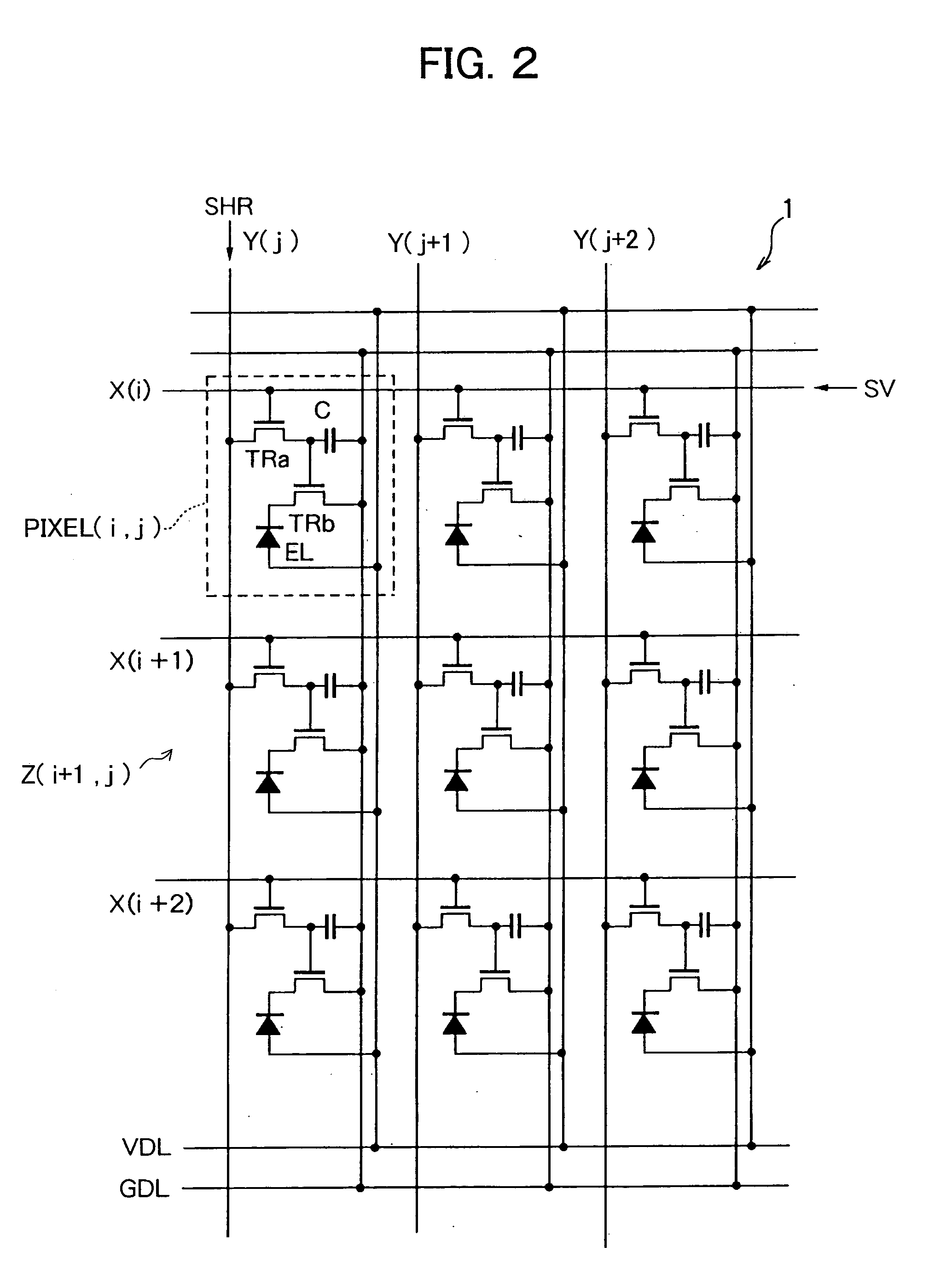
[0050]FIG. 1 is a block diagram showing the configuration of an organic EL display device of the present embodiment. FIG. 2 is a circuit diagram showing the configuration of pixels of the present embodiment.

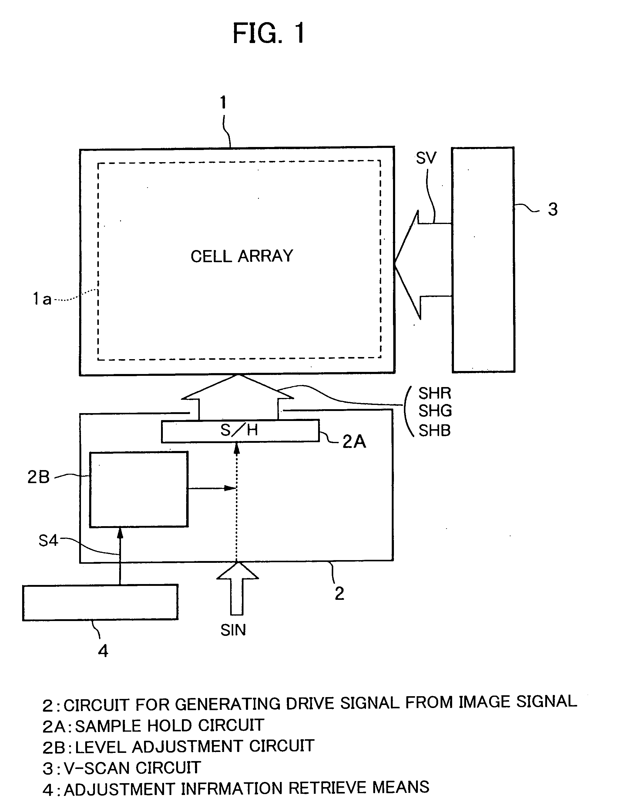
[0051] The display device illustrated in FIG. 1 comprises a cell array 1 wherein a large number of pixels including an organic EL element provided at each of cross points of a plurality of scan lines in the line direction and a plurality of data lines in the column direction are arranged in matrix in a predetermined color arrangement, and a signal processing and data line drive circuit 2 connected to data lines in accordance with an input address signal, for performing necessary signal processing on an input image signal and supplying to the data lines of the cell array 1.

[0052] Also, the display device comprises a scan line drive (V-scan) circuit 3 connected to the scan lines, for applying a scan signal SV to scan lines at a predetermined period.

[0053] In the cell array 1 sho...

second embodiment

[0061] In the second embodiment, a detailed configuration of a display device and a method of adjusting color balance fluctuated when produced will be explained.

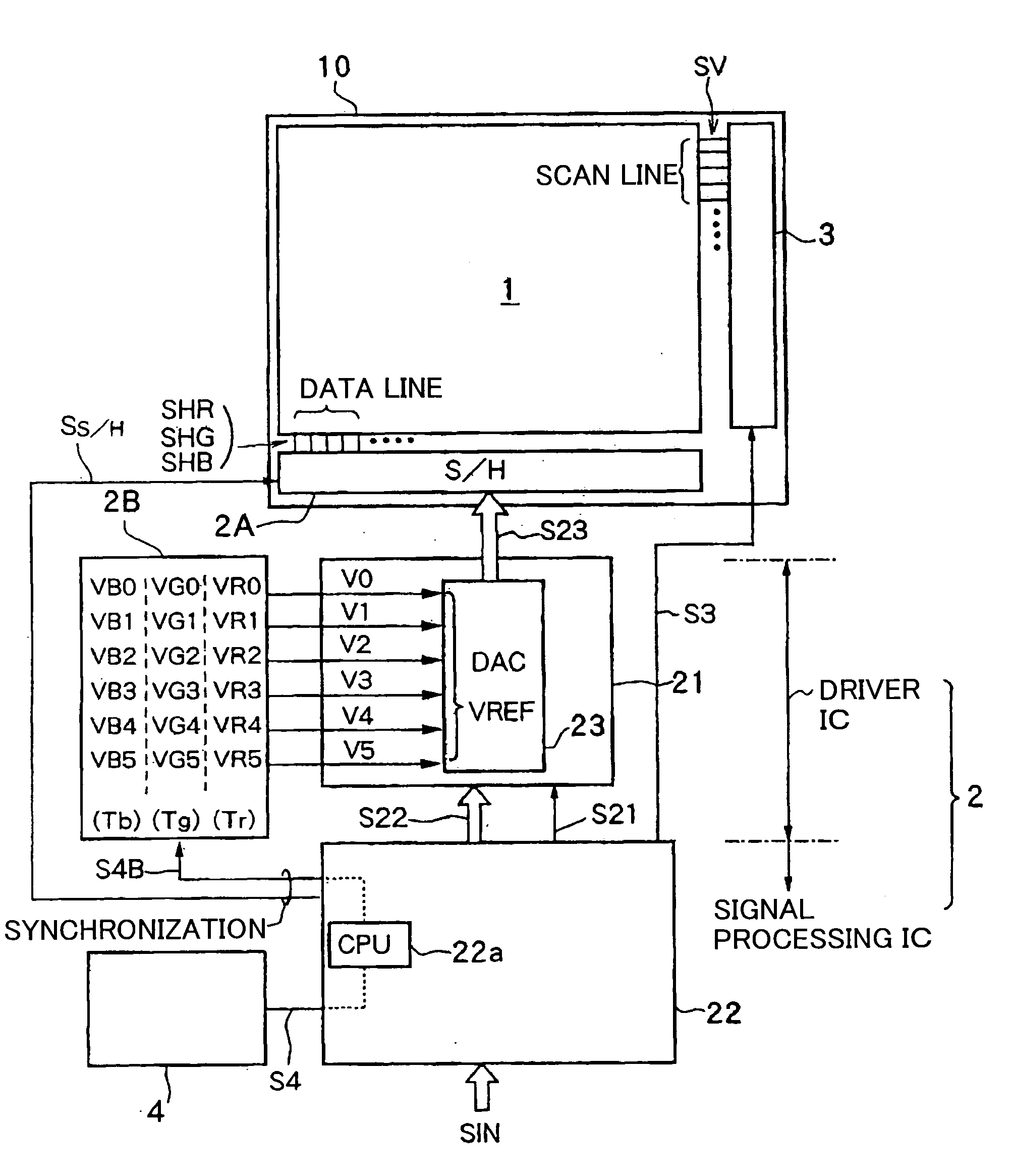
[0062]FIG. 3 is a block diagram of a display device showing a detailed configuration example of the configuration in FIG. 1.

[0063] In the display device shown in FIG. 3, a sample hold circuit 2A for generating a data line drive signal and a V-scan circuit 3 are provided inside a display panel 10 together with the cell array 1. A signal processing circuit 22 and a driver IC are provided on a circuit substrate outside of the display panel 10.

[0064] The signal processing circuit 22 performs necessary digital signal processing, such as, resolution conversion, IP (Interlace-Progressive) conversion and noise removal, on an input image signal SIN.

[0065] The driver IC converts an image signal (digital signal) after signal processing to an analog signal and performs parallel-serial conversion. A serial-analog RGB signal after the...

third embodiment

[0099] In the third embodiment, potential of an anode or a cathode of an organic EL element (hereinafter, referred to as an EL voltage) is detected, and a suitable drive voltage for each of the RGB signals based on the result is output. The detection result of the EL voltage corresponds to “information relating to light emission adjustment” in the first embodiment. Since it is possible to always monitor this information, luminance of the respective RGB colors can be automatically corrected in accordance with changes of characteristics of the organic EL element over time.

[0100] Below, the third embodiment will be explained by taking as an example the case of detecting an anode voltage of organic EL elements and automatically correcting changes over time based on the result.

[0101] Since organic EL elements are self-luminous elements, the luminance declines due to thermal fatigue of the organic multilayer body when emitting light at high luminance for a long time.

[0102]FIG. 10 is a ...


PUM


Abstract

A circuit for generating drive signals (SHR, SHG and SHB) from an input image signal (SIN), a cell array (1) including a light emitting element (EL) for emitting light of a predetermined color of red (R), green (G) or blue (B) by being applied with a drive signal (SHR, SHG and SHB) supplied for each color from the circuit (2), an adjustment information retrieve means (4) for obtaining information relating light emission adjustment of the light emitting element (EL), and a level adjustment circuit (2B) provided in the circuit (2) for changing a level of an RGB signal (S22) before divided to drive signals (SHR, SHG and SHB) for the respective RGB colors based on the information obtained by the adjustment information retrieve means (4) are provided. In the present invention, color balance adjustment can be performed by the above small scale circuit.

Description

TECHNICAL FIELD [0001] The present invention relates to an image display device wherein a pixel has a light emitting element for emitting light in accordance with a luminance level of an image signal to be input and a luminance adjustment method thereof. BACKGOUND ART [0002] In an image display device having fixed pixels, since the most popular liquid crystal display at present needs a backlight, a light emission amount of the backlight has to be increased to obtain higher luminance of a displayed image. However, when the light emission amount of the backlight is increased, although the luminance of the displayed image becomes high but the contrast becomes poor because the light cannot be completely blocked by the liquid crystal. Namely, luminance and contrast of a displayed image are in a trade-off relationship in a liquid crystal display, so that it is difficult to balance the both at high levels. [0003] As an image display device for eliminating the problem, there is known an ima...

Claims


Application Information

Patent Timeline
Patent Type & Authority Applications(United States)
IPC IPC(8): G09G3/20H05B33/12G09G3/30G09G3/32H01L51/50
CPCG09G3/2092G09G2360/16G09G3/3241G09G2300/0842G09G2310/0251G09G2310/0262G09G2310/027G09G2320/0242G09G2320/0261G09G2320/0276G09G2320/029G09G2320/043G09G2320/045G09G2320/048G09G2320/0626G09G2320/066G09G2320/0666G09G2320/103G09G2330/021G09G2330/028G09G2360/144G09G3/3233G09G3/30G09G3/20
Inventor TAMURA, MITSUYASUHASEGAWA, HIROSHI
Owner JOLED INC
Why Eureka
Try Eureka