

Method of fabricating crystalline silicon and switching device using crystalline silicon
a technology of crystalline silicon and crystalline silicon, which is applied in the field of crystallizing amorphous silicon, can solve the problems of reducing the display quality of an lcd device, the surface of silicon film is apt to oxidize at its top surface, etc., and achieves the reduction and the effect of reducing the formation or elimination of non-uniform portions in a semiconductor layer
- Summary
- Abstract
- Description
- Claims
- Application Information
AI Technical Summary
Benefits of technology
Problems solved by technology
Method used
Image

Examples
first embodiment
[0045]FIGS. 3A to 3C illustrate schematic plane views showing a process of fabricating a semiconductor layer of crystalline silicon according to the invention.
[0046]FIG. 3A shows a buffer layer 112 and a semiconductor layer 114 of amorphous silicon that are sequentially formed on a substrate 110 having a first region “IIIa” and a second region “IIIb” at the periphery of the first region “IIIa.”
[0047]FIG. 3B shows an alignment key 116 that is formed at each corner portion in the second region “IIIb” of the substrate 110 by crystallizing a portion of the semiconductor layer 114 of amorphous silicon. Accordingly, the semiconductor layer 114 corresponding to the alignment key 116 of the second region “IIIb” crystallizes, but the semiconductor layer 114 in other portions of the second region “IIIb” does not crystallize. For example, the alignment key 116 of crystalline silicon has a shape of “” in the first embodiment. The alignment key 116 may have various shapes such as “,”“S,”“E,”“,”“...
second embodiment
[0054]FIGS. 5A to 5D are schematic plane views showing a process of fabricating a semiconductor layer of crystalline silicon according to the invention.
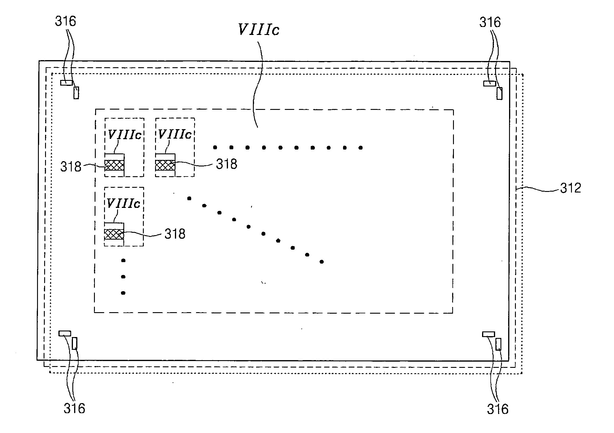
[0055]FIG. 5A shows a buffer layer 312 and an amorphous silicon semiconductor layer 314 that are sequentially formed on a substrate 310 having a first region “VIIIa” and a second region “VIIIb” at the periphery of the first region “VIIIa.”
[0056]FIG. 5B shows that a portion of the semiconductor layer 314 in the second region “VIIIb” is removed to form an alignment key 316 by irradiating a laser beam having an energy density higher than the energy corresponding to a complete melting regime. This technique of removing silicon may be referred to as an ablation.
[0057] Generally, when a laser beam irradiates onto a semiconductor layer, an energy density band of the laser beam may divide into four regimes according to the state of the semiconductor layer directly after irradiation: i) a partial melting regime, ii) a nearly complete melting...
PUM
 Abstract
Description
Claims
Application Information