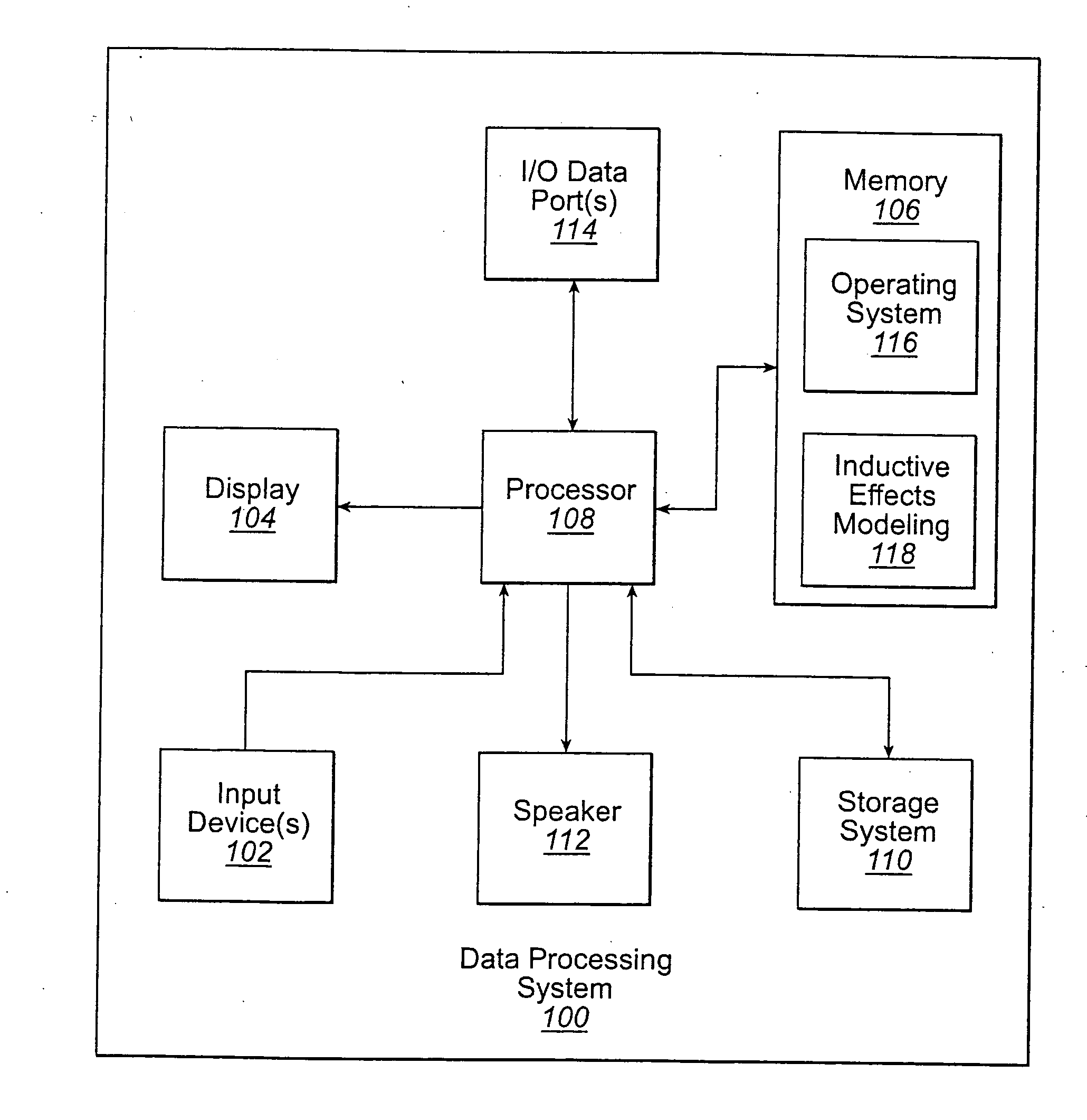
Methods, systems, and computer program products for modeling inductive effects in a circuit by combining a plurality of localized models
a technology of inductive effects and localized models, applied in the field of electromagnetic modeling of integrated circuits and systems, can solve the problems of computational cost, inability to apply additional approximations and simplifications, and inability to efficiently extract and analyze the localization of magnetic couplings,
- Summary
- Abstract
- Description
- Claims
- Application Information
AI Technical Summary
Benefits of technology
Problems solved by technology
Method used
Image

Examples
examples
A. Single Layer 2×128 Bit Bus
FIG. 10 illustrates a bus consisting of two blocks of 128 lines (W 1 μm, H 2 pin, Sp 1 μm, L 1000 μm) with a 16 μm gap between the two blocks. The driver resistance RDr is 70 Ω and the load capacitance CLd is 2 fF. Every sixteenth line is a return line (no driver resistance).
In FIGS. 11A-11D the far end node voltage responses for two lines of the bus are shown for 1V step and 10 ps ramp inputs. The far end response reduces in magnitude with increasing distance from the active line. The reference results (white circles) are obtained by including all individual couplings, which results in relatively high runtimes and memory consumption (see Table 1). Double-inverse inductance models are sparsified as described above, dependent on cutoff percentage (the smaller, the more accurate). For simple truncation, all off-diagonals are set to zero, which are zero for the double-inverse model with the given cutoff threshold to ensure fair comparison of the efficie...
PUM
 Abstract
Description
Claims
Application Information
 - R&D
- Intellectual Property
- Life Sciences
- Materials
- Tech Scout
- Unparalleled Data Quality
- Higher Quality Content
- 60% Fewer Hallucinations
Browse by: Latest US Patents, China's latest patents, Technical Efficacy Thesaurus, Application Domain, Technology Topic, Popular Technical Reports.
© 2025 PatSnap. All rights reserved.Legal|Privacy policy|Modern Slavery Act Transparency Statement|Sitemap|About US| Contact US: help@patsnap.com