Group III nitride based flip-chip integrated circuit and method for fabricating

a technology of flip-chip integrated circuits and nitride, which is applied in the direction of printed circuit aspects, basic electric elements, solid-state devices, etc., can solve the problems of low electron mobility, high source resistance, and serious degrading of the high performance gain otherwise possibl

Inactive Publication Date: 2005-03-31
CREE INC
View PDF13 Cites 80 Cited by
  • Summary
  • Abstract
  • Description
  • Claims
  • Application Information

AI Technical Summary

Benefits of technology

[0016] In another flip-chip integrated circuit configuration, a circuit substrate including an insulating material, has passive circuit elements on a first surface. A Group III nitride active semiconductor device is flip-chip mounted on the circuit substrate and is electrically connected to the passive circuit element.

Problems solved by technology

One disadvantage of Si is that it has low electron mobility (approximately 1450 cm2 / V-s), which produces a high source resistance.
This resistance seriously degrades the high performance gain otherwise possible from Si based FETs.
However, GaAs has a relatively small bandgap (1.42 eV at room temperature) and relatively small breakdown voltage, which prevents GaAs based HEMTs from providing high power.
One disadvantage of sapphire substrates is that they have poor thermal conductivity and the total power output of devices formed on sapphire substrates can be limited by the substrate's thermal dissipation.
Sapphire substrates are also difficult to etch.
SiC substrates have higher thermal conductivity (3.5-5 w / cmk) but have the disadvantages of being relatively expensive and not available in large wafer diameters of 4-inch and greater.
This reduced yield adds to the cost of fabricating Group III transistors on SiC substrates.
One disadvantage of these wafers is that they cannot be easily used as a substrate for Group-III nitride based devices because the lattice mismatch between the materials leads to poor quality semiconductor devices.
Another disadvantage of these wafers is that they have low thermal conductivity.
In some instances GaAs semiconductor devices may not have the necessary operating characteristics.
For example, a GaAs based multistage amplifier may not be able to provide the required output power levels.
However, such an implementation has some disadvantages.
First, the area required for a multi-stage MMIC with interstage networks and all the passive circuit elements is large.
Second, device and circuit models of GaN transistors are less established than their GaAs counterparts, thus making it difficult to accurately design and yield multistage GaN amplifiers that provide higher gain and power outputs.

Method used


Image

  • Group III nitride based flip-chip integrated circuit and method for fabricating
  • Group III nitride based flip-chip integrated circuit and method for fabricating
  • Group III nitride based flip-chip integrated circuit and method for fabricating

Examples


Embodiment Construction

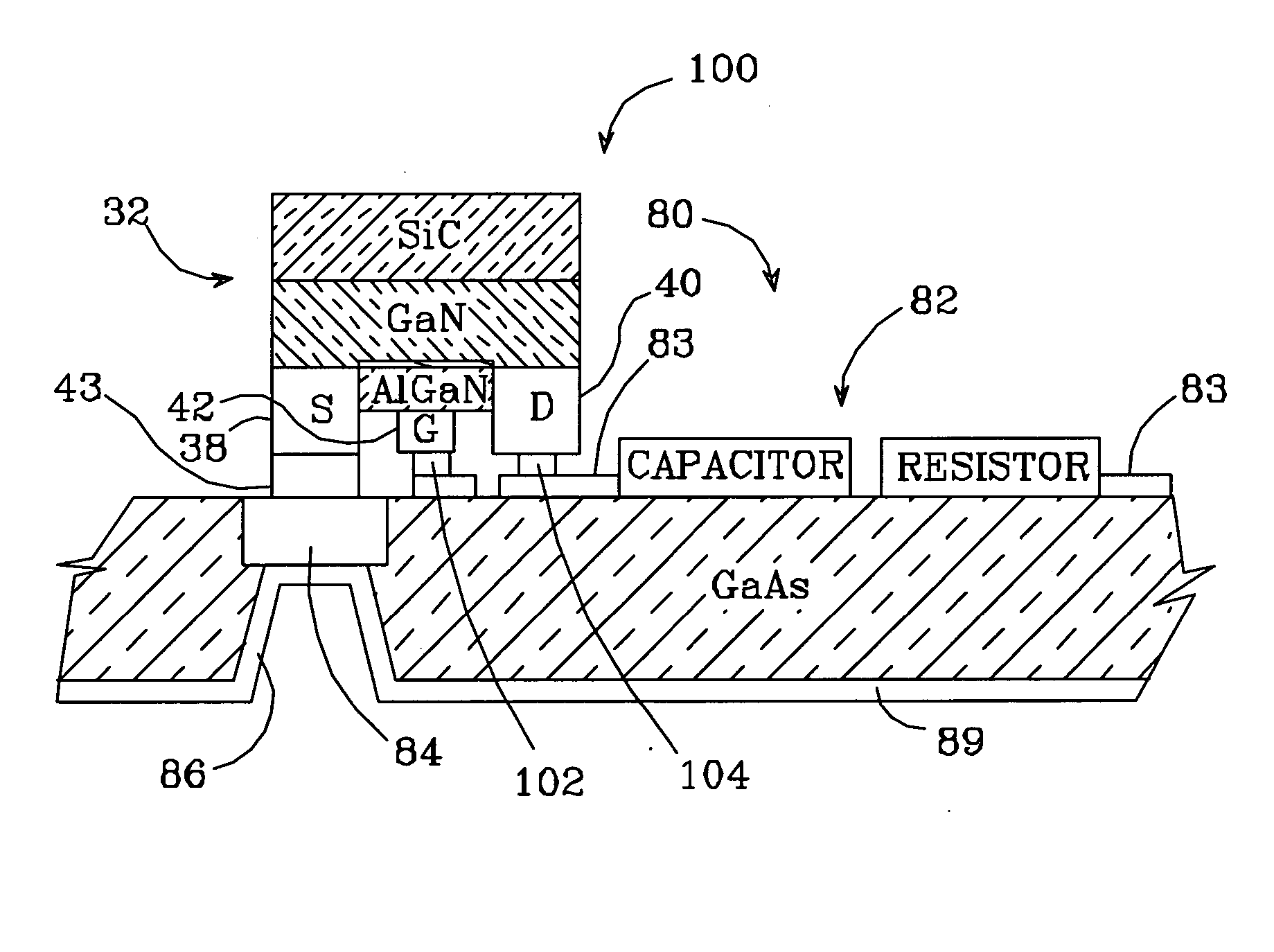
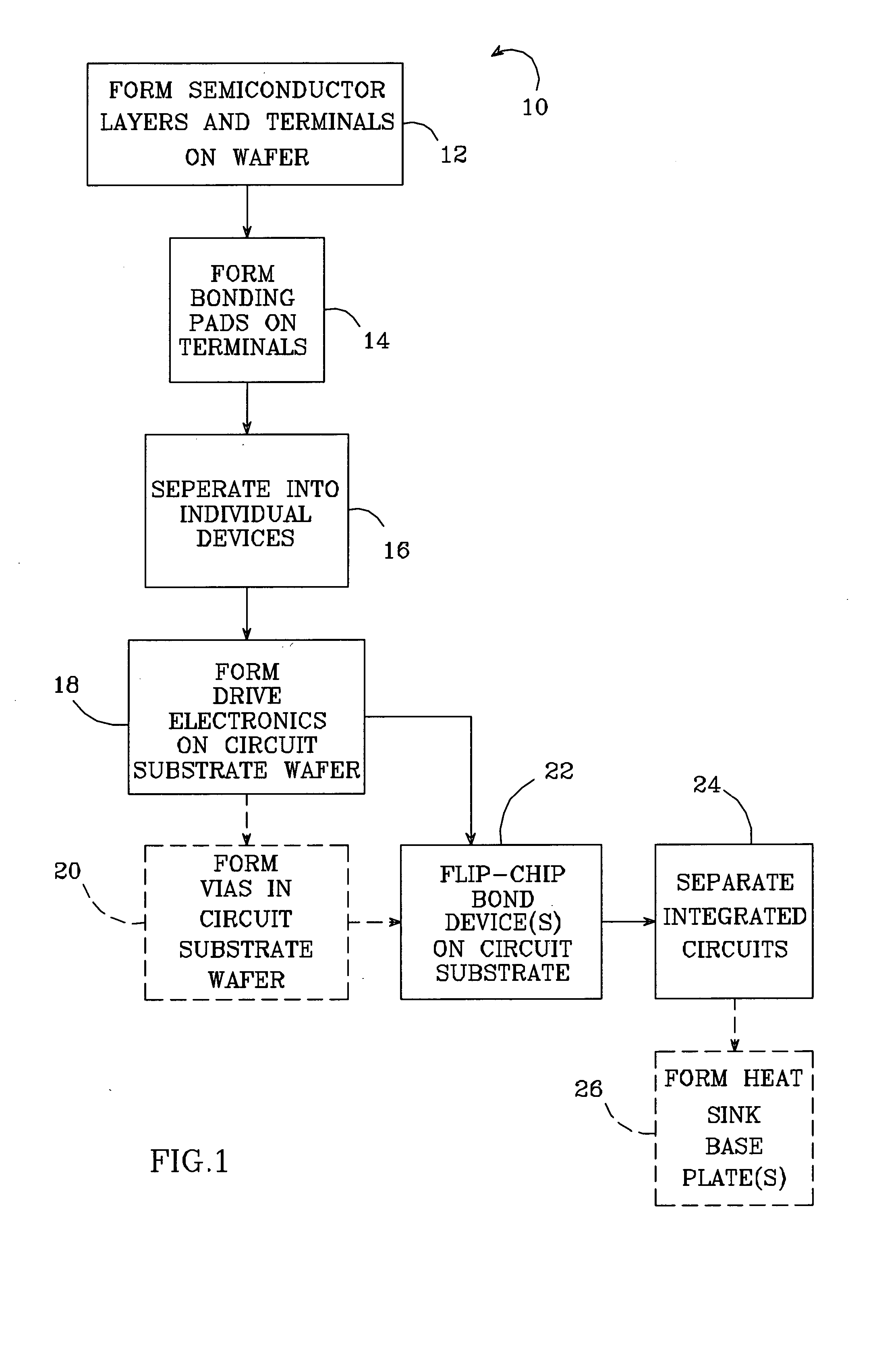
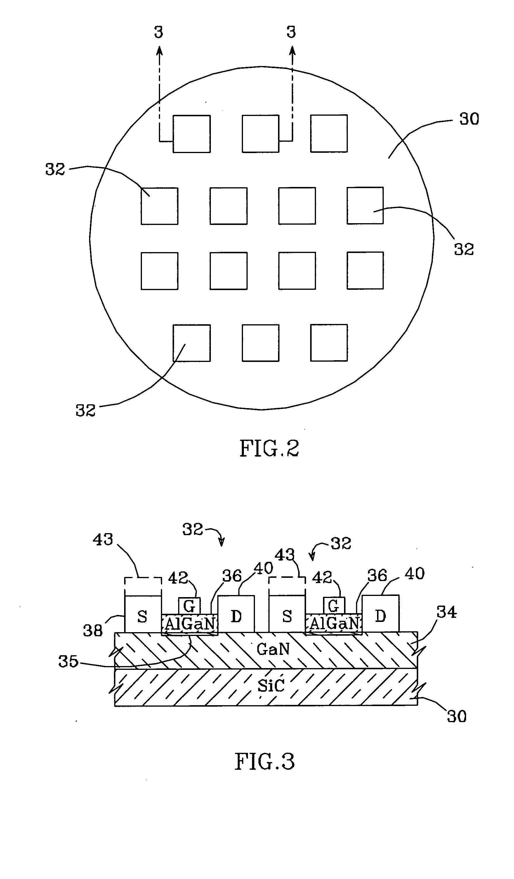
[0035]FIG. 1 shows one embodiment of a method 10 according to the present invention. In the first step 12, semiconductor layers of a semiconductor device and device terminals are formed on a wafer. A preferred semiconductor device is a Group III nitride based device such as an AlGaN HEMT or FET grown on a sapphire, SiC, GaN, AlN or Si wafer, with the preferred wafer being a 4 H polytype of SiC. Other SiC polytypes can also be used including 3C, 6H and 15R polytypes. An AlxGa1-xN buffer layer (where x in between 0 and 1) can be included between the wafer and device active layers to provide an appropriate crystal structure transition between the SiC wafer (substrate) and the active layers.

[0036] Generally, SiC wafers are preferred over sapphire and Si because they have a much closer crystal lattice match to Group III nitrides, which results in Group III nitride films of higher quality. SiC also has a very high thermal conductivity so that the total output power of Group III nitride d...


PUM

PropertyMeasurementUnit
diameteraaaaaaaaaa
diametersaaaaaaaaaa
thickaaaaaaaaaa

Abstract

A circuit substrate has one or more active components and a plurality of passive circuit elements on a first surface. An active semiconductor device has a substrate with layers of material and a plurality of terminals. The active semiconductor device is flip-chip mounted on the circuit substrate and at least one of the terminals of the device is electrically connected to an active component on the circuit substrate. The active components on the substrate and the flip-chip mounted active semiconductor device, in combination with passive circuit elements, form preamplifiers and an output amplifier respectively. In a power switching configuration, the circuit substrate has logic control circuits on a first surface. A semiconductor transistor flip-chip mounted on the circuit substrate is electrically connected to the control circuits on the first surface to thereby control the on and off switching of the flip-chip mounted device.

Description

RELATED APPLICATIONS [0001] This is a continuation-in-part of application Ser. No. 10 / 335,915, filed Jan. 2, 2003.BACKGROUND OF THE INVENTION [0002] 1. Field of the Invention [0003] This invention relates to semiconductor devices, and more particularly to semiconductor devices that are flip-chip mounted on circuit substrates having passive components and / or active components. [0004] 2. Description of Related Art [0005] Microwave systems commonly use solid state transistors as amplifiers and oscillators, which has resulted in significantly reduced system size and increased reliability. To accommodate the expanding number of microwave systems, there is an interest in increasing their operating frequency and power. Higher frequency signals can carry more information (bandwidth), allow for smaller antennas with very high gain, and provide radar with improved resolution. [0006] Field effect transistors (FETs) and high electron mobility transistors (HEMTs) are common solid state transisto...

Claims


Application Information

Patent Timeline
Patent Type & Authority Applications(United States)
IPC IPC(8): H01L21/8252H01L23/14H01L23/367H01L23/66H01L27/06H01L29/20H01L29/778
CPCH01L21/8252Y10T29/4913H01L23/3677H01L23/66H01L27/0605H01L29/2003H01L29/7787H01L2224/16235H01L2224/16238H01L2224/1703H01L2224/73253H01L2924/01002H01L2924/01004H01L2924/01013H01L2924/01015H01L2924/01029H01L2924/01042H01L2924/01074H01L2924/01075H01L2924/01078H01L2924/01079H01L2924/10329H01L2924/14H01L2924/1423H01L2924/19011H01L2924/19041H01L2924/19042H01L2924/19043H01L2924/19105H01L2924/30105H01L23/147H05K2201/066H05K1/181H05K1/0206H01L23/367H01L2924/19103H01L2924/01087H01L2924/0002H01L2924/12032H01L2924/00H01L25/00H01L27/00
Inventor MISHRA, UMESHPARIKH, PRIMITWU, YIFENG
Owner CREE INC
Why Eureka
Try Eureka