Flat panel display

Active Publication Date: 2005-04-14
SAMSUNG DISPLAY CO LTD
View PDF5 Cites 6 Cited by
  • Summary
  • Abstract
  • Description
  • Claims
  • Application Information

AI Technical Summary

Benefits of technology

[0008] Accordingly, in exemplary embodiments of the present invention, a high-speed flat panel display having a long lifetime is provided. The flat panel display has a pixel portion and driving circuit portions that are com

Problems solved by technology

However, because an on-current is very high, the amount of a current flowing through EL elements in the pixel portion exceeds a limit value, and thus luminance per unit area increases, which shortens the lifetime of the EL elements.
Further, when the pixel portion and the driving portions are composed of thin film tr

Method used


Image

  • Flat panel display
  • Flat panel display
  • Flat panel display

Examples


Example

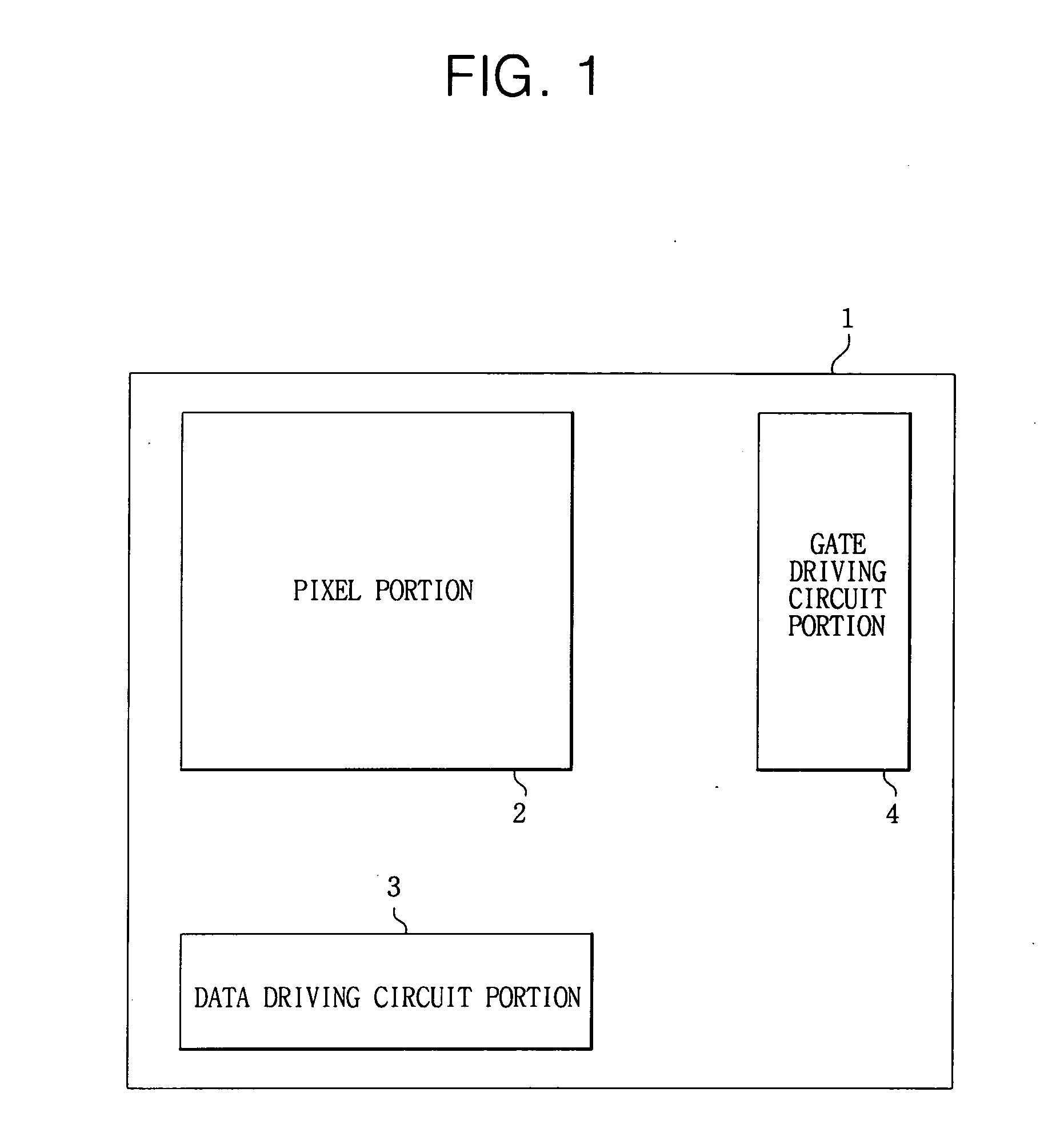
[0026] Referring to FIG. 1, an OLED display device includes a pixel portion 2 in which a plurality of pixels are arranged in a matrix form, and driving circuit portions for driving the pixel portion 2 on an insulating substrate 1. Although the pixel portion 2 is not shown in detail in FIG. 1, a plurality of gate lines, a plurality of data lines, a plurality of power lines, and a plurality of pixels connected to the lines are arranged in a matrix form. Each pixel is basically composed of an electroluminescent (EL) element, a driving transistor for supplying a driving current according to a data signal from a data line to the EL element, a switching transistor for delivering the data signal to the driving transistor in response to a scan signal applied to a gate line, a capacitor for storing the data signal, and the like.

[0027] The driving circuit portions for driving the pixels in the pixel portion 2 include a gate driving circuit portion 4 for providing a scan signal for driving th...


PUM


Abstract

A high-speed flat panel display having a long lifetime. Thin film transistors in a pixel portion having a plurality of pixels are contacted differently from thin film transistors in driving circuit portions for driving the pixels, thereby enhancing luminance uniformity and reducing power consumption. The thin film transistors each have a channel region and a body contact region for applying a predetermined voltage to the channel region. At least one thin film transistor in the pixel portion is a source-body contact thin film transistor having the body contact region connected to one of source and drain electrodes so that the predetermined voltage can be provided to the channel region. Each thin film transistor in the driving circuit portion is a gate-body contact thin film transistor having the body contact region connected to the gate electrode so that a predetermined voltage can be provided to the channel region.

Description

CROSS-REFERENCE TO RELATED APPLICATION [0001] This application claims priority to and the benefit of Korean Patent Application No. 2003-64895, filed Sep. 18, 2003 in the Korean Intellectual Property Office, the disclosure of which is incorporated herein by reference in its entirety. BACKGROUND OF THE INVENTION [0002] 1. Field of the Invention [0003] The present invention relates to a flat panel display and, more particularly, to a high-speed flat panel display having a long lifetime in which thin film transistors of a pixel portion and driving circuit portions have different body contact structures. [0004] 2. Description of the Related Art [0005] Generally, an active matrix organic light emitting diode (AMOLED) display includes a pixel portion in which an array of thin film transistors is arranged, and a data driving circuit portion and a gate driving circuit portion for driving the array of thin film transistors in the pixel portion. [0006] In a conventional AMOLED display, the thi...

Claims


Application Information

Patent Timeline
IPC IPC(8): H01L27/12H01L51/50H01L27/32H01L29/78H01L29/786H05B33/00
CPCH01L27/12H01L27/3262H01L29/78639H01L29/78615H01L29/783H10K59/1213H05B33/00
Inventor KOO, JAE-BONCHOI, BYOUNG-DEOG
Owner SAMSUNG DISPLAY CO LTD
Why Eureka
Try Eureka