Liquid crystal display panel device and method of fabricating the same

a technology of liquid crystal display and panel device, which is applied in the direction of semiconductor devices, instruments, optics, etc., can solve the problems of increasing the manufacturing cost of the lcd panel device, complicated four-round mask process, and limited cost reduction, so as to reduce the number of mask processes

Active Publication Date: 2005-04-14
LG DISPLAY CO LTD
View PDF13 Cites 28 Cited by
  • Summary
  • Abstract
  • Description
  • Claims
  • Application Information

AI Technical Summary

Benefits of technology

[0023] An object of the present invention is to provide an LCD panel device fabricated using a reduced number of mask processes.
[0024]...

Problems solved by technology

Fabrication of the lower array substrate includes relatively complicated fabrication processes, such as various semiconductor processes that require a plurality...

Method used


Image

  • Liquid crystal display panel device and method of fabricating the same
  • Liquid crystal display panel device and method of fabricating the same
  • Liquid crystal display panel device and method of fabricating the same

Examples


Embodiment Construction

[0051] Reference will now be made in detail to the preferred embodiments of the present invention, examples of which are illustrated in the accompanying drawings.

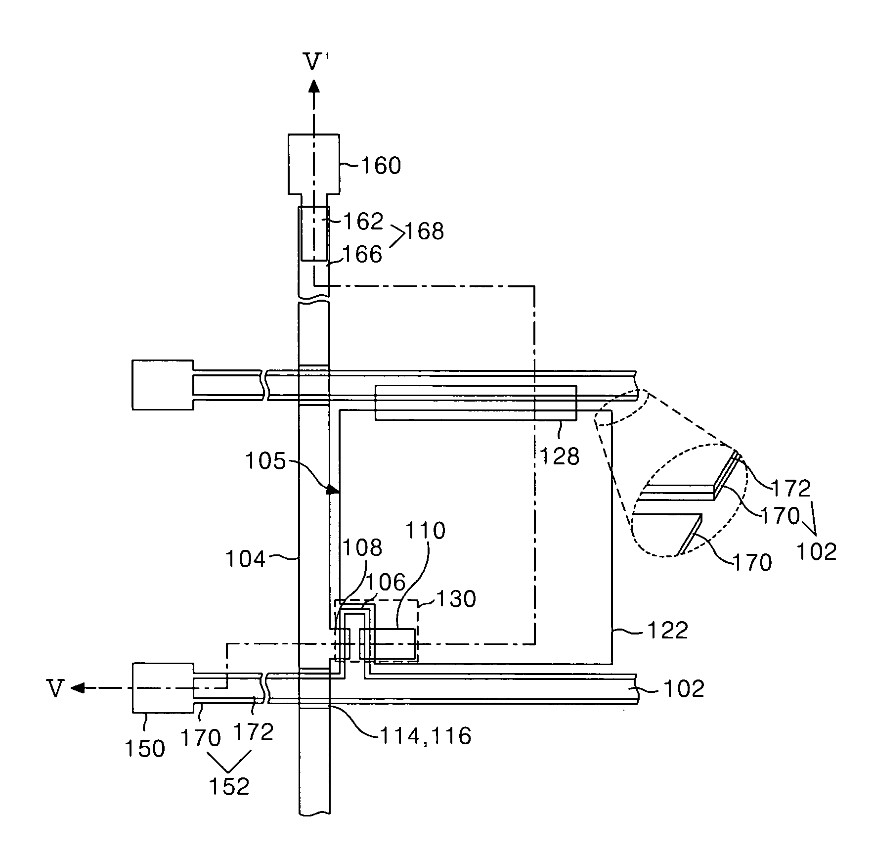
[0052]FIG. 4 is a plan view of an exemplary lower array substrate of an LCD panel device according to the present invention, and FIG. 5 is a cross sectional view of the lower array substrate along V-V′ of FIG. 4 according to the present invention. In FIGS. 4 and 5, a lower array substrate may include a gate line 102 and a data line 104 provided on a lower substrate 101 in such a manner to intersect each other with having a gate insulating pattern 112 therebetween, a TFT 130 provided at each of the intersections, a pixel electrode 122 provided at a pixel area 105 defined by the intersections, a storage capacitor 140 provided at an overlapping portion between the pixel electrode 122 and the gate line 102, a gate pad 150 extending from the gate line 102, and a data pad 160 extending from the data line 104. The gate line 102 m...


PUM


Abstract

A liquid crystal display panel device includes a thin film transistor array substrate having a gate line provided on a substrate, a data line intersecting the gate line and having a gate insulating pattern disposed therebetween to define a pixel area, a thin film transistor provided at the intersection between the gate line and the data line, a protective film for protecting the thin film transistor, a pixel electrode provided at the pixel area and connected to the thin film transistor, a gate pad connected to the gate line and formed from a transparent conductive film included in the gate line, and a data pad connected to the data line and formed from the transparent conductive film, and a color filter array substrate joined with the thin film transistor array substrate to be opposed to each other, wherein the protective film is provided at an area where it overlaps with the color filter array substrate to expose the transparent conductive films included in the gate pad and the data pad.

Description

[0001] The present invention claims the benefit of Korean Patent Application No. P2003-71377, filed in Korea on Oct. 14, 2003, which is hereby incorporated by reference. BACKGROUND OF THE INVENTION [0002] 1. Field of the Invention [0003] The present invention relates to a liquid crystal display (LCD) device and a method of fabricating an LCD device, and more particularly to an LCD panel device and a fabricating method of fabricating an LCD panel device. [0004] 2. Description of the Related Art [0005] In general, an LCD device controls transmission of light through liquid crystal material by application of an electric field thereto, thereby displaying an image. The LCD device drives the liquid crystal material by varying the electric field formed between a pixel electrode and a common electrode arranged in opposition to each other on upper and lower substrates. [0006] The LCD device includes a lower array substrate (i.e., thin film transistor (TFT) array substrate) and an upper array...

Claims


Application Information

Patent Timeline
IPC IPC(8): G02F1/136G02F1/1362
CPCG02F2001/136231G02F1/1362G02F1/136231G02F1/136
Inventor YOO, SOON SUNGCHANG, YOUN GYOUNGNAM, SEUNG HEE
Owner LG DISPLAY CO LTD
Why Eureka
Try Eureka