Thin film transistor array substrate and fabricating method thereof, liquid crystal display using the same and fabricating method thereof, and method of inspecting liquid crystal display

a thin film transistor array and substrate technology, applied in the direction of semiconductor devices, semiconductor/solid-state device details, instruments, etc., can solve the problems of undetectable complexity and cost, four-mask process can still be undetectable and costly, and achieve the effect of facilitating contact of automatic inspection pins

Inactive Publication Date: 2005-04-14
LG DISPLAY CO LTD
View PDF11 Cites 27 Cited by
  • Summary
  • Abstract
  • Description
  • Claims
  • Application Information

AI Technical Summary

Benefits of technology

[0033] An advantage of the present invention provides a thin film transistor array substrate and method of fabricating the same in a reduced number of mask processes, a liquid crystal display using the same and a fabricating method thereof, and a method of inspecting the liquid crystal display.
[0034] Another advantage of the present invention provides a thin film transistor array substrate and method of fabricating the same in a reduced number of mask processes, a liquid crystal display using the same and a fabricating method thereof, and a method of inspecting the liquid crystal display that facilitates contact of an automatic inspecting pin during an automated inspection process.

Problems solved by technology

The process used to fabricate the TFT array substrate described above is complicated and relatively expensive because it involves a number of semiconductor processing techniques that require a plurality of mask processes.
While the TFT array substrate described above may be formed using a four-mask process that is advantageous over previously known five-mask processes, the four-mask process can still be undesirably complicated and, therefore, costly.

Method used


Image

  • Thin film transistor array substrate and fabricating method thereof, liquid crystal display using the same and fabricating method thereof, and method of inspecting liquid crystal display
  • Thin film transistor array substrate and fabricating method thereof, liquid crystal display using the same and fabricating method thereof, and method of inspecting liquid crystal display
  • Thin film transistor array substrate and fabricating method thereof, liquid crystal display using the same and fabricating method thereof, and method of inspecting liquid crystal display

Examples


first embodiment

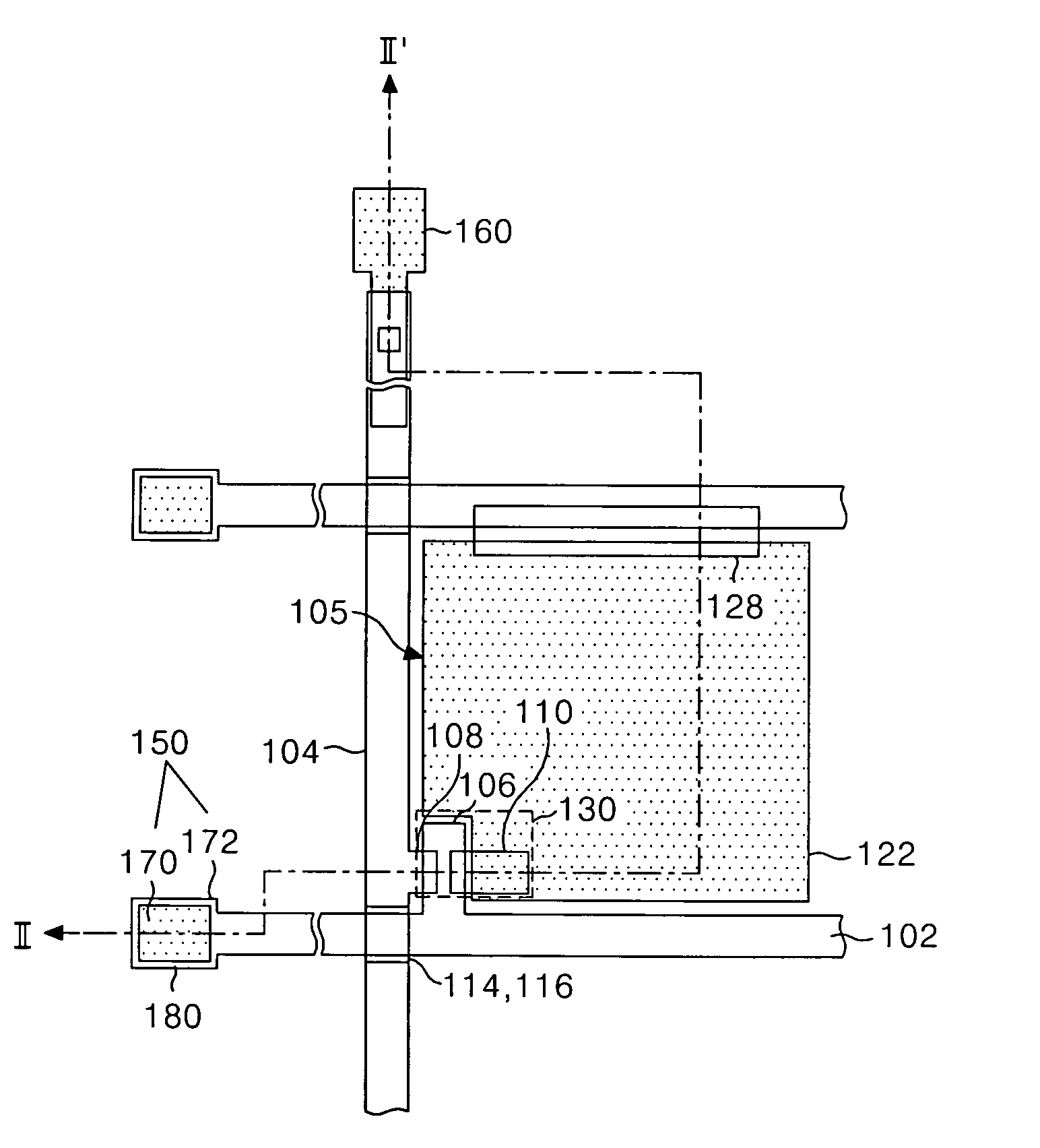
[0128]FIG. 4 illustrates a plan view of a TFT array substrate according to the present invention. FIG. 5 illustrates a sectional view of the TFT array substrate taken along line II-II′ shown in FIG. 4.

[0129] Referring to FIGS. 4 and 5, the TFT array substrate of the first embodiment may, for example, include gate lines 102 and data lines 104 formed so as to cross each other on a lower substrate 101 and to define a plurality of pixel areas 105; a gate insulating pattern 112 formed between the gate and data lines 102 and 104; a thin film transistor 130 at each crossing of the gate and data lines 102 and 104; a pixel electrode 122 at each pixel area, a storage capacitor 140 provided at a region where a storage electrode 128 and gate line 102 overlap, a gate pad 150 extending from the gate line 102, and a data pad 160 extending from the data line 104.

[0130] Each gate line 102 may be supplied with a gate signal, each data line 104 may be supplied with a data signal. In response to a gat...

second embodiment

[0159]FIG. 11 illustrates a plan view of a TFT array substrate according to the present invention. FIG. 12 illustrates a sectional view of the TFT array substrate taken along line 111-111′ shown in FIG. 11.

[0160] The TFT array substrate shown in FIGS. 11 and 12, and its method of fabrication, is, in many respects, similar to the TFT array substrate shown in FIGS. 4 and 5 but is different with respect to the gate pad. Thus, for the sake of brevity, a detailed explanation of elements similar to both the second and first embodiments will be omitted.

[0161] Referring to FIGS. 11 and 12, gate signals may be supplied to each gate line 102 via a corresponding gate pad 150. Accordingly, the gate pad 150 may be connected to a gate driver (not shown) that supplies gate signals. In one aspect of the present invention, the gate line 102 may comprise the transparent conductive material 170 and the overlaying gate metal material 172. In another aspect of the present invention, the gate pad 150 ma...

third embodiment

[0180]FIG. 18 illustrates a plan view of a TFT array substrate according to the present invention. FIG. 19 illustrates a sectional view of the TFT array substrate taken along line VI-VI′ shown in FIG. 18.

[0181] The TFT array substrate shown in FIGS. 18 and 19, and its method of fabrication, is, in many respects, similar to the TFT array substrate shown in FIGS. 4 and 5 but is different with respect to the pixel electrode, the gate pad, an upper gate pad electrode, the data pad, a lower data pad electrode, an upper data pad electrode. Thus, for the sake of brevity, a detailed explanation of elements similar to both the third and first embodiments will be omitted.

[0182] Referring to FIGS. 18 and 19, the pixel electrode 272 may be provided directly on a lower substrate 288. In one aspect of the present invention, the pixel electrode 272 may, for example, directly contact a portion of a drain electrode 262 of a thin film transistor 280 exposed by a protective film pattern 298. During o...


PUM

PropertyMeasurementUnit
widthaaaaaaaaaa
widthaaaaaaaaaa
widthaaaaaaaaaa

Abstract

A TFT array substrate is fabricated in a reduced number of processes. The TFT array substrate includes gate and data pads with enlarged contact areas to facilitate contact with an inspecting pin of an inspection device. An LCD incorporating the TFT array substrate is inspected by contacting the inspecting pin to the gate and data pads. The TFT array substrate includes first, second, and third conductive pattern groups. The first conductive pattern group includes a gate electrode, a gate line, and a lower gate pad electrode. The second conductive pattern group includes source and drain electrodes, a data line, and a lower data pad electrode. The third conductive pattern group includes a pixel electrode, and upper gate and data pad electrodes. A semiconductor pattern is along and beneath the second conductive pattern group. Gate insulating and protective film patterns are at areas not occupied by the third conductive pattern group.

Description

[0001] This application claims the benefit of Korean Patent Application Nos. P2003-71400, P2003-92698, P2003-98823, and P2003-100989, filed on Oct. 14, 2003, Dec. 17, 2003, Dec. 29, 2003, and Dec. 30, 2003, respectively, which are hereby incorporated by reference for all purposes as if fully set forth herein. BACKGROUND OF THE INVENTION [0002] 1. Field of the Invention [0003] The present invention relates to a liquid crystal display (LCD) device and methods of fabricating the same. More particularly, the present invention relates to a thin film transistor (TFT) array substrate for an LCD device and a method of fabricating the same in a reduced number of mask processes. Further, the present invention relates to a method of inspecting LCD device. More particularly, the present invention relates to a method of fabricating a TFT array substrate that facilitates an inspection process. [0004] 2. Discussion of the Related Art [0005] Liquid crystal display (LCD) devices express pictures by ...

Claims


Application Information

Patent Timeline
Patent Type & Authority Applications(United States)
IPC IPC(8): G02F1/1368G02F1/1335G02F1/1343G02F1/1345G02F1/136G02F1/1362H01L21/00H01L21/3205H01L23/52H01L29/786
CPCG02F1/136227G02F2001/136254G02F2001/136231G02F1/136286G02F1/136231G02F1/136254
Inventor LIM, BYOUNG HOYOO, SOON SUNGLEE, CHANG DEOKNAM, SEUNG HEEOH, JAE YOUNGKIM, HONG SIKKWACK, HEE YOUNG
Owner LG DISPLAY CO LTD
Why Eureka
Try Eureka