
Method and memory system in which operating mode is set using address signal
a memory system and address signal technology, applied in the field of memory systems, can solve the problems of reducing the effective operating speed of the memory system, inefficient repetition of mrs commands,
- Summary
- Abstract
- Description
- Claims
- Application Information
AI Technical Summary
Benefits of technology
Problems solved by technology
Method used
Image

Examples
Embodiment Construction
[0043] The present invention will now be described in detail with reference to preferred but non-limiting embodiments of the invention.
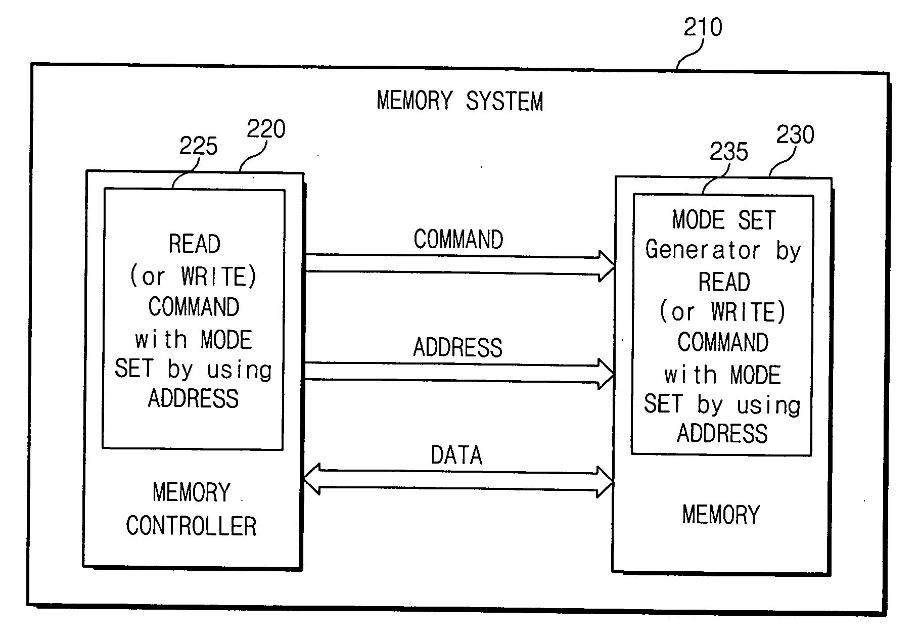
[0044]FIG. 6 shows a block diagram of a first embodiment of a memory system 210. The memory system 210 includes a memory controller 220 and a memory device 230. As explained in further detail below, the memory controller includes unit 225 for generating and communicating an operating mode parameter using a multi-bit address signal transmitted together with the READ or WRITE command. Meanwhile, the memory device 230 includes a mode set generator 235 for setting an operating mode of the memory device 230 in accordance with an operating mode parameter received via the address lines during a data read or write operation.
[0045]FIG. 7 shows a data processing block diagram of a first embodiment of a memory device 230. The memory device 230 includes input buffers 40, 55, Mode Register Set (MRS) Generator 60, Command Decoder 70, Row Address Buffer 80, Colum...
PUM
 Abstract
Description
Claims
Application Information