Manufacturing method of optical device provided with resin thin film having micro-asperity pattern

a manufacturing method and resin thin film technology, applied in the direction of identification means, instruments, photomechanical equipment, etc., can solve the problems of uneven exposure amount, lowered processing precision, blurred exposed region, etc., and achieve satisfactory processing accuracy

Inactive Publication Date: 2005-04-14
ORMON CORP
View PDF3 Cites 16 Cited by
  • Summary
  • Abstract
  • Description
  • Claims
  • Application Information

AI Technical Summary

Benefits of technology

[0010] The present invention was made in view of the above problems and it is an object of the present invention to provide a manufacturing method of an optical device having a micro-asperity pattern, which can form various kinds of three-dimensional shapes with satisfactory processing accuracy.

Problems solved by technology

However, in this conventional method, when ultraviolet rays and the like are applied with a mask in photolithography, since the rays are diffused in the photosensitive resin material because of the micro-asperity pattern formed on the surface of the photosensitive material, there are problems such that 1) an exposed region is blurred and processing precision is lowered and 2) an exposed amount becomes uneven and a development defect is generated.

Method used


Image

  • Manufacturing method of optical device provided with resin thin film having micro-asperity pattern
  • Manufacturing method of optical device provided with resin thin film having micro-asperity pattern
  • Manufacturing method of optical device provided with resin thin film having micro-asperity pattern

Examples


embodiment 1

[0033] [Embodiment 1]

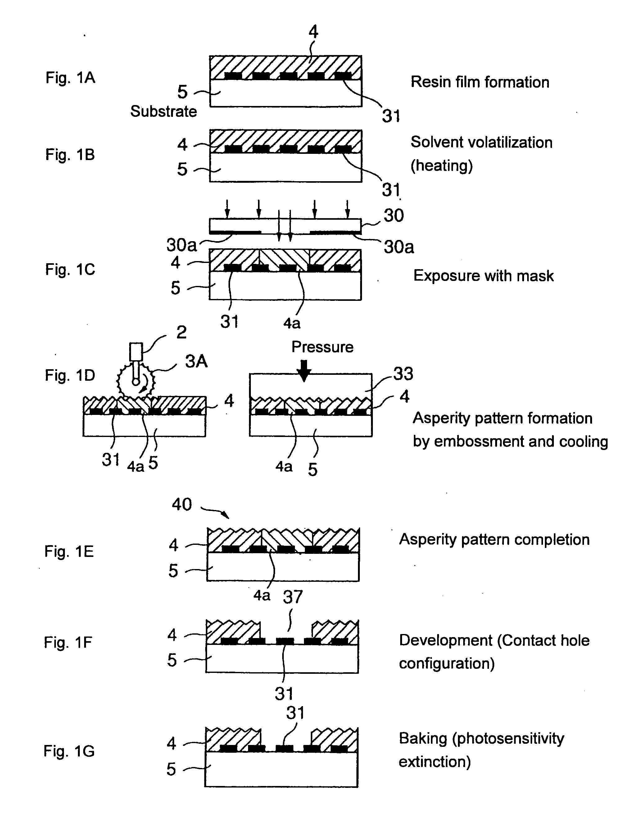
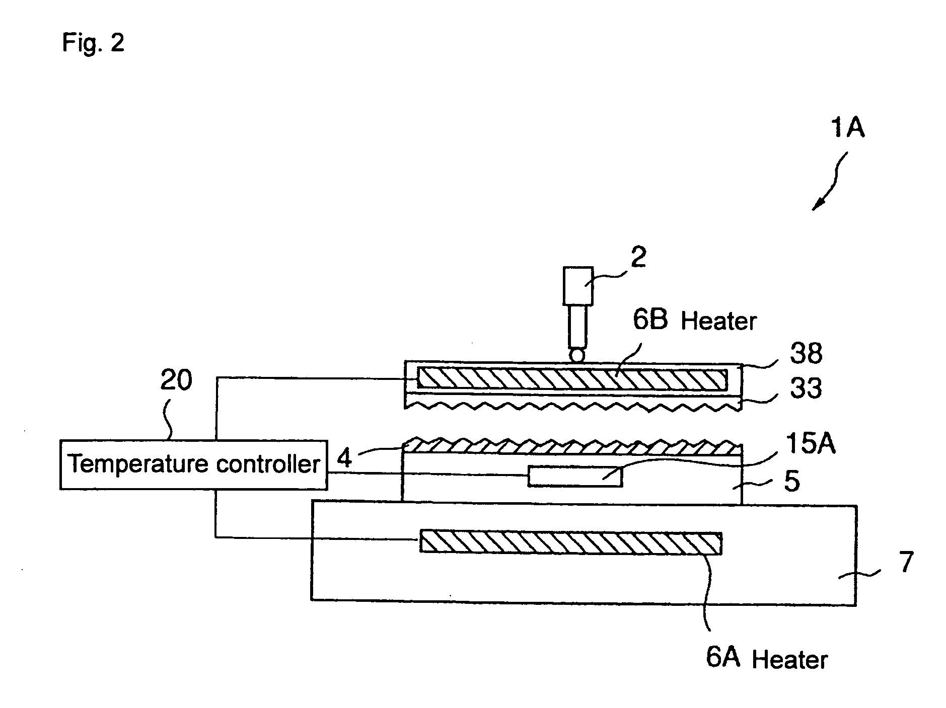
[0034]FIG. 1 shows a manufacturing method of an optical device according to an embodiment of the present invention. As shown in FIG. 1A, a resin thin film 4 is formed of a photosensitive resin such as an acrylic resin by spin coating on a glass substrate 5 on which an electronic device 31 such as liquid-crystal driving element TFTs or a wiring contact 31 or the like and then as shown in FIG. 1B, unnecessary solvent is volatized by heating the resin thin film 4. Then, as shown in FIG. 1C, unnecessary parts of a transmission material 30 is covered with a mask 30a and irradiated with ultraviolet rays to form a material-property-changed part 4a in which properties of the material is changed. In this state, the glass substrate 5 is heated by a hot plate while it is controlled such that the resin thin film 4 and the material-property-changed part 4a are kept at a temperature lower than either a photosensitivity extinction temperature or a hardening reaction starting t...

embodiment 2

[0047] [Embodiment 2]

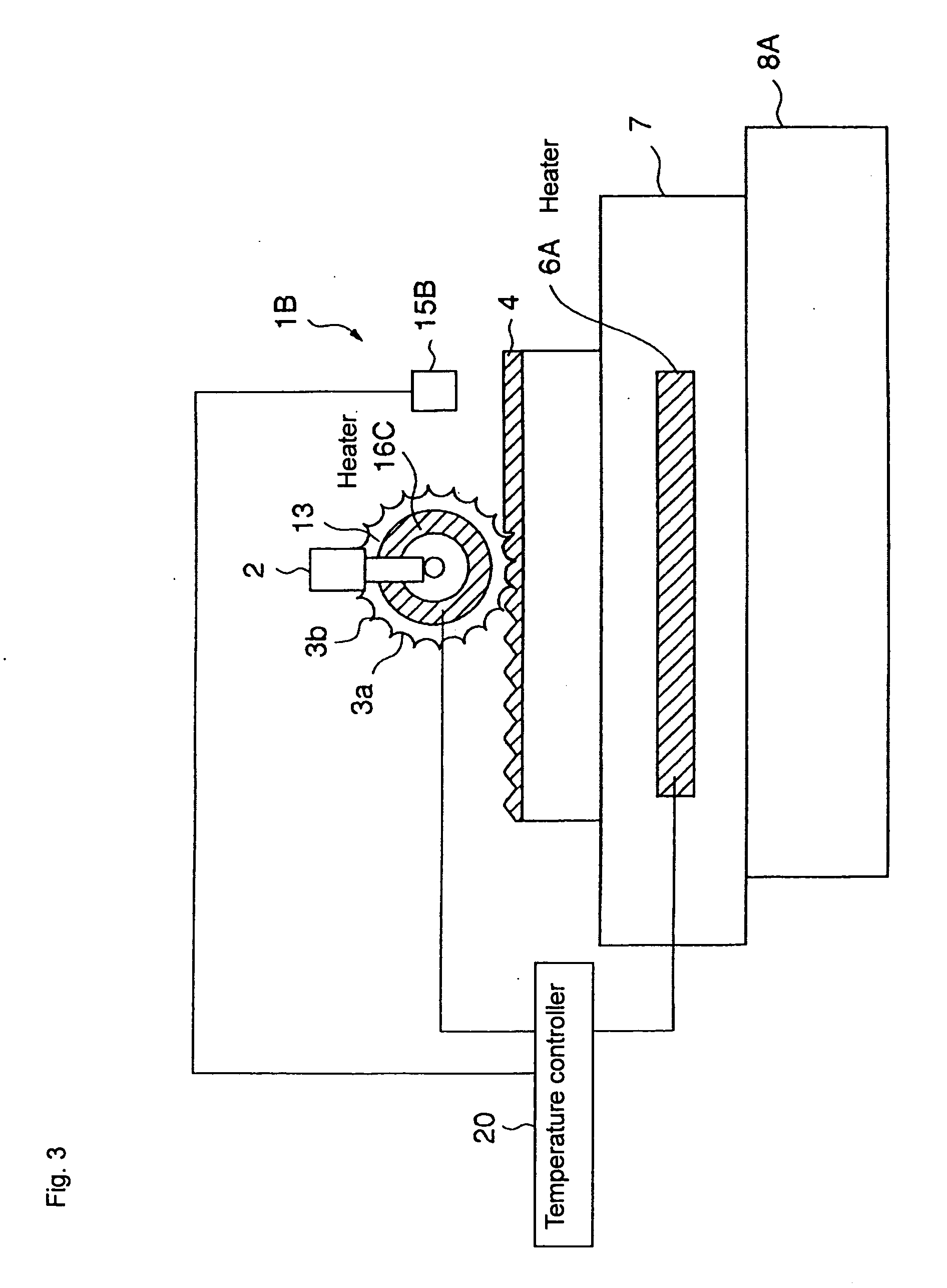
[0048]FIG. 3 shows a main part of a micro-asperity pattern forming apparatus 1B according to a second embodiment of the present invention. This embodiment is different from the first embodiment in that an embossment roll 13 has a cylindrical configuration, a heater 16C is provided inside the embossment roll 13, the heater 16C and a heater 6A provided inside a transfer stage 7 can be controlled by a temperature controller 20 and a resin thin film 4 is heated while the resin thin film 4 is pressed by the embossment roll 13.

[0049] According to the second embodiment, the heater 16C is provided inside the embossment roll 13 so as to be able to heat the embossment roll 13 from the inside, and the heater 6A is provided inside the transfer stage 7. These heaters are controlled by the temperature controller 20 based on a detection temperature by a temperature sensor 15B. The heaters may be a heating wire heater, a high-power lamp, a ceramic heater or the like. Theses he...

embodiment 3

[0052] [Embodiment 3]

[0053]FIG. 4 shows a main part of a micro-asperity pattern forming apparatus 1C according to a third embodiment of the present invention. This embodiment is different from the first embodiment shown in FIG. 2 in that an elastic body 10 such as a synthetic rubber, a rectangular metal sheet or a combination of those is interposed between a base 38 and the stamper 33. Thus, even when there is a manufacturing error such as undulation in the base 38 or the stamper 33, since it can be absorbed, an optical device can be manufactured with high precision. In addition, heaters 6A and 6B are not indicated for convenience of explanation.


PUM

PropertyMeasurementUnit
depthaaaaaaaaaa
temperatureaaaaaaaaaa

Abstract

A manufacturing method of an optical device having a micro-asperity pattern that has various kinds of accurate three-dimensional shapes and is realized as thin films includes: a first step of coating a substrate with a resin thin film made of a photosensitive resin; a second step of forming a material-property-changed part at a part of the resin thin film by photolithography; a third step of controlling a temperature of the resin thin film to be a temperature that is lower than a photosensitivity extinction temperature or a hardening reaction starting temperature of the resin thin film; a fourth step of pressing a die having a micro-asperity pattern against the surface of the resin thin film to form a first micro-asperity pattern in a state in which the resin thin film has been softened or melted; and a fifth step of forming a second micro-asperity pattern at a part of the resin thin film by removing the material-property-changed part.

Description

BACKGROUND OF INVENTION [0001] 1. Field of the Invention [0002] The present invention relates to a manufacturing method of an optical device provided with a resin thin film having a micro-asperity pattern. [0003] 2. Background Art [0004] In this specification, “optical device” is a device which has at least a micro-asperity pattern on its surface and diffuses, condenses and reflects light, “micro-asperity pattern” is a generic term of asperity shapes that develop one-dimensionally or two-dimensionally and are 0.1 μm to hundreds of micrometers in depth and arbitrary in width, length and shape. In addition, “electronic device” is a generic term of electronic circuit constitutions for displaying pixels comprising pixel driving elements such as thin film transistors (TFTs), metal wiring contacts or the like. [0005] Recently, as a liquid crystal display such as a personal computer, a TV, a word processor, a video equipment or the like, reflection-type liquid crystal display that displays...

Claims


Application Information

Patent Timeline
Patent Type & Authority Applications(United States)
IPC IPC(8): B29C39/10B29C39/22B29C59/02B29C59/04B29D11/00B29L11/00G02B1/04G02B5/02G02B5/08G02F1/1335G03F7/38G09F9/30
CPCB29C43/021Y10T428/24917B29C43/226B29C43/3697B29C59/026B29C59/046B29C2043/463B29C2059/023B29D11/00B29L2011/00B29L2011/0016G02B5/021G02B5/0215G02B5/0268G02B5/0284G02F1/133553G03F7/38B29C43/222G02F2203/03
Inventor IKEDA, MASAAKIAOYAMA, SHIGERU
Owner ORMON CORP
Why Eureka
Try Eureka