Etching method and method of manufacturing circuit device using the same
a manufacturing method and circuit device technology, applied in the direction of photosensitive material processing, printed circuit non-printed electric components association, double exposure, etc., can solve the problems of small etching factor value of the above-described etching method, significant erosion in the side direction of etching, and reduce current capacity thereby, so as to improve the etching factor
- Summary
- Abstract
- Description
- Claims
- Application Information
AI Technical Summary
Benefits of technology
Problems solved by technology
Method used
Image
Examples
first embodiment
(First Embodiment for Describing an Etching Method)
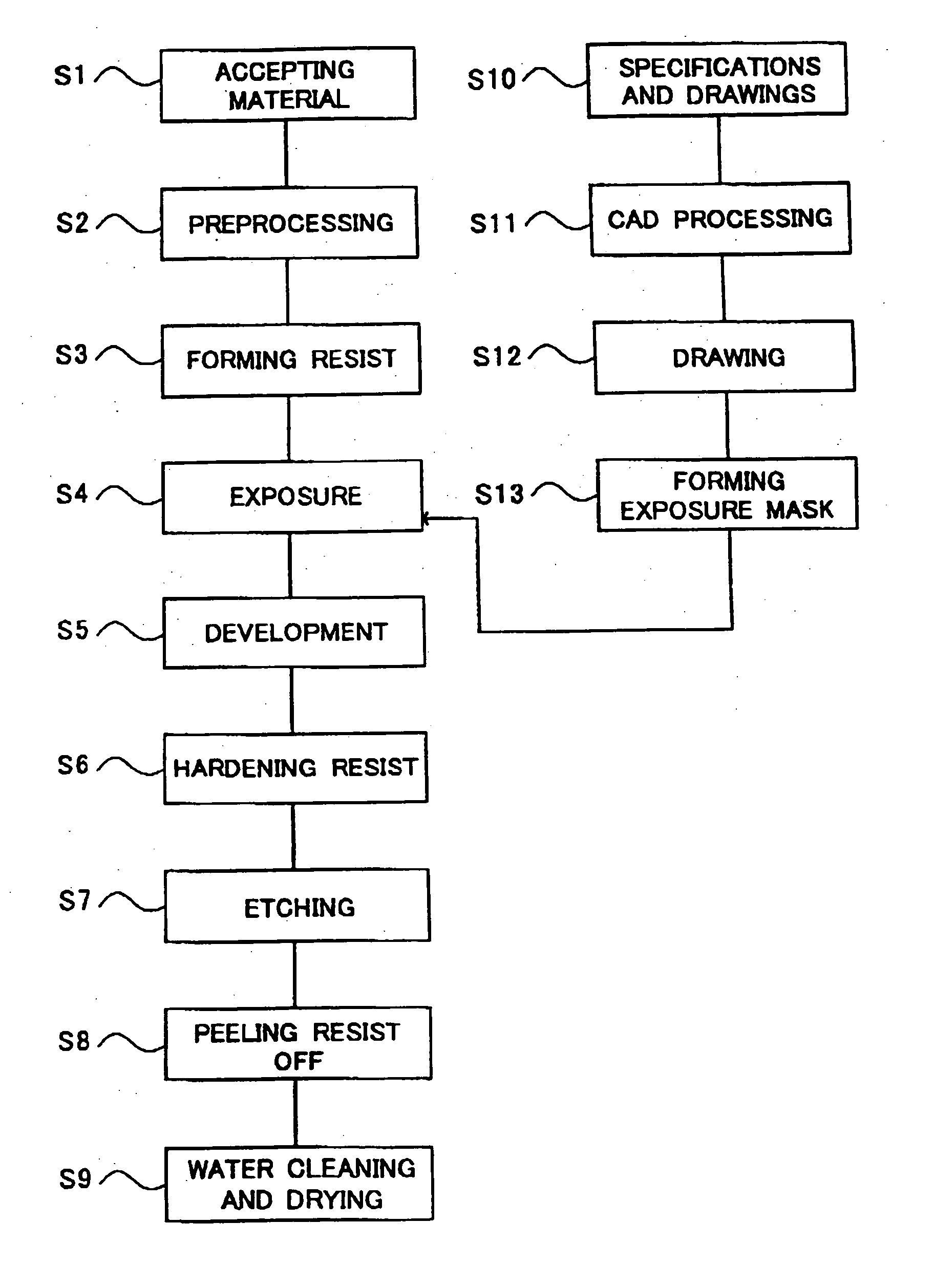
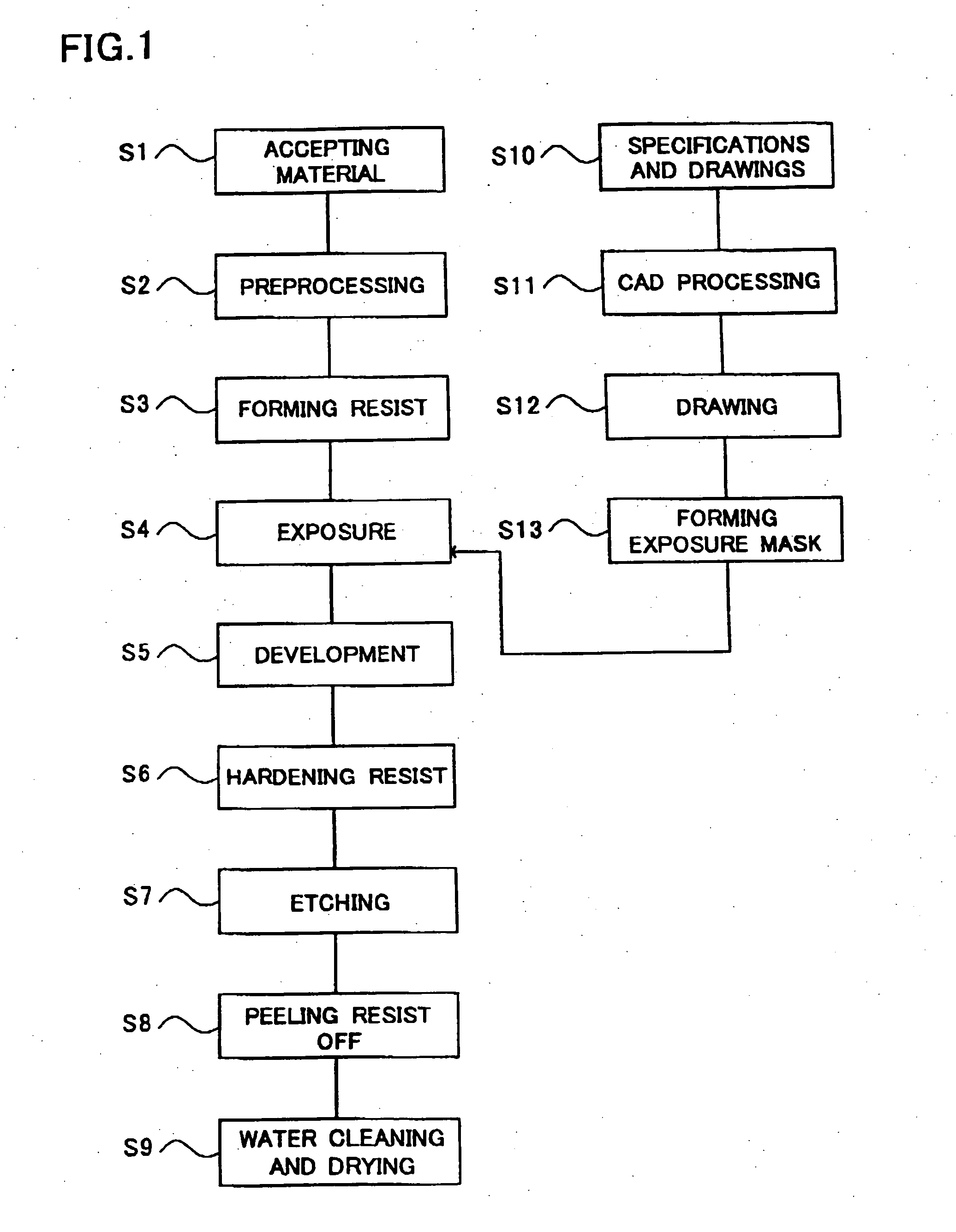
[0024] Firstly, an outline of an etching method of a preferred embodiment will be described with reference to a flowchart of FIG. 1.
[0025] First, in Step S1, an etching material subject to etching (an etching target material) is accepted. The material to be accepted herein may include a sheet of conductive foil made of metal, a laminated sheet in which a plurality of sheets of conductive foil are laminated with an insulating layer therebetween, a board applying a conductive foil on a surface thereof, and the like. Then, in Step S2, dust and oily components attached to a surface of the etching target material are removed as preprocessing.
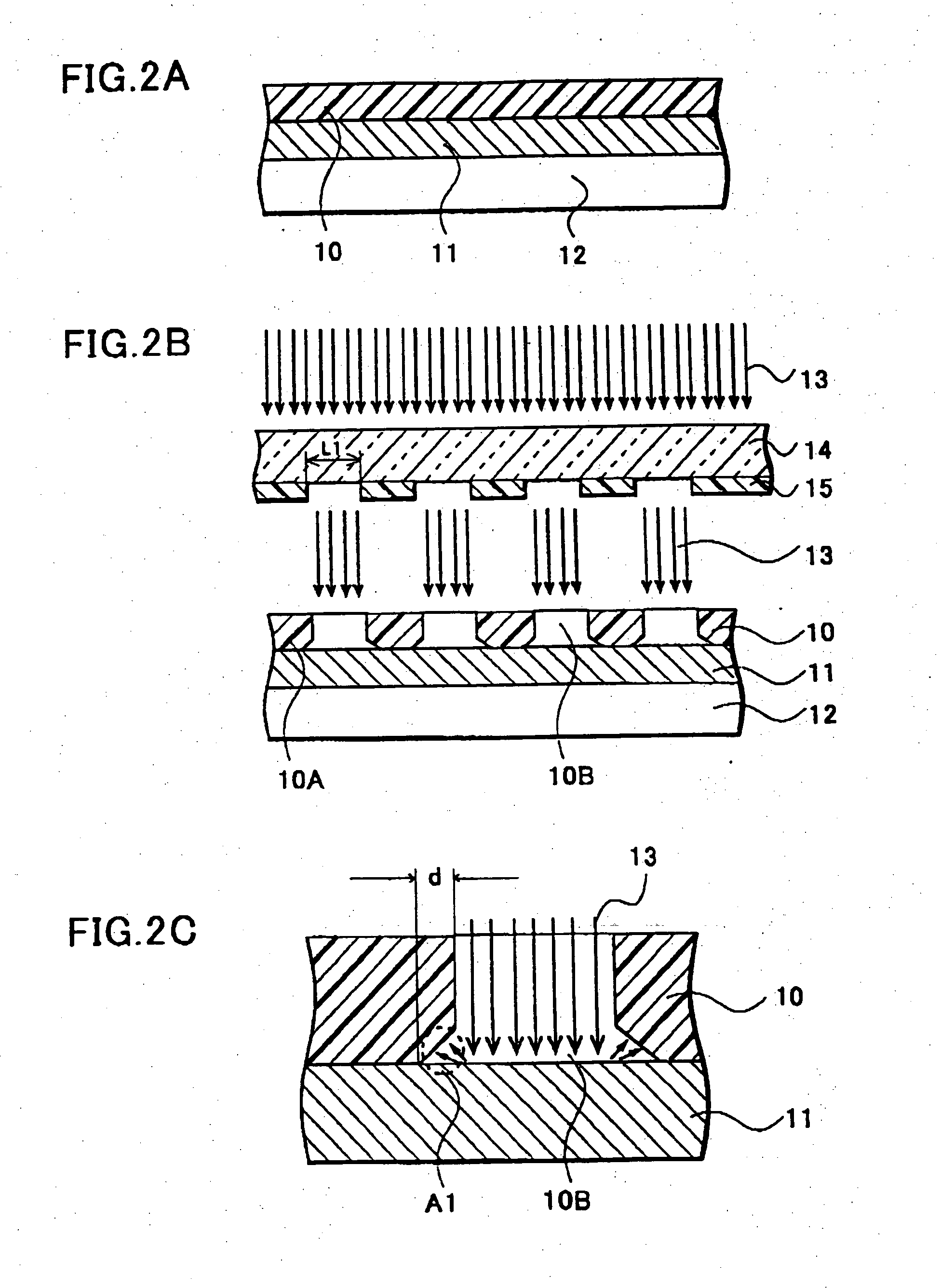
[0026] In Step S3, a resist is formed on the surface of the etching target material. This resist can be formed by means of coating a liquid resist or laminating a resist of a sheet type (DFR). The resist used herein is either a negative resist or a positive resist. In Step 4, the coated resist is s...
second embodiment
(Second Embodiment for Describing a Method of Manufacturing a Circuit Device)
[0050] Next, several types of circuit devices manufactured by use of the above-described etching method will be introduced with reference to FIGS. 5A to 5C. Configurations of circuit devices 20A to 20C according to another preferred embodiment of the present invention will be described with reference to FIGS. 5A to 5C. FIG. 5A to FIG. 5C are cross-sectional views of circuit devices of respective modes.
[0051] Referring to FIG. 5A, a circuit device 20A of the preferred embodiment of the present invention includes a conductive pattern 21, a circuit element 22 die bonded to the conductive pattern 21 through solder, and an external electrode 27 as connecting means for electrically connecting the conductive pattern 21 to the outside.
[0052] The conductive pattern 21 is made of a metal such as copper, and is buried in sealing resin 28 while exposing a rear surface thereof. Meanwhile, respective conductive pattern...
PUM
| Property | Measurement | Unit |
|---|---|---|
| conductive | aaaaa | aaaaa |
| thickness | aaaaa | aaaaa |
| current capacity | aaaaa | aaaaa |
Abstract
Description
Claims
Application Information


