Level shifter and flat panel display

Inactive Publication Date: 2005-06-09
SAMSUNG SDI CO LTD
View PDF4 Cites 0 Cited by
  • Summary
  • Abstract
  • Description
  • Claims
  • Application Information

AI Technical Summary

Benefits of technology

[0011] It is an aspect of the present invention

Problems solved by technology

Also, power consumption is increased when the NMOS transistors MN1 and MN2 are turned off

Method used


Image

  • Level shifter and flat panel display
  • Level shifter and flat panel display
  • Level shifter and flat panel display

Examples


Embodiment Construction

[0025] In the following detailed description, only certain exemplary embodiments of the present invention are shown and described, simply by way of illustration. As those skilled in the art would realize, the described embodiments may be modified in various different ways, all without departing from the spirit or scope of the present invention. Accordingly, the drawings and description are to be regarded as illustrative in nature, and not restrictive.

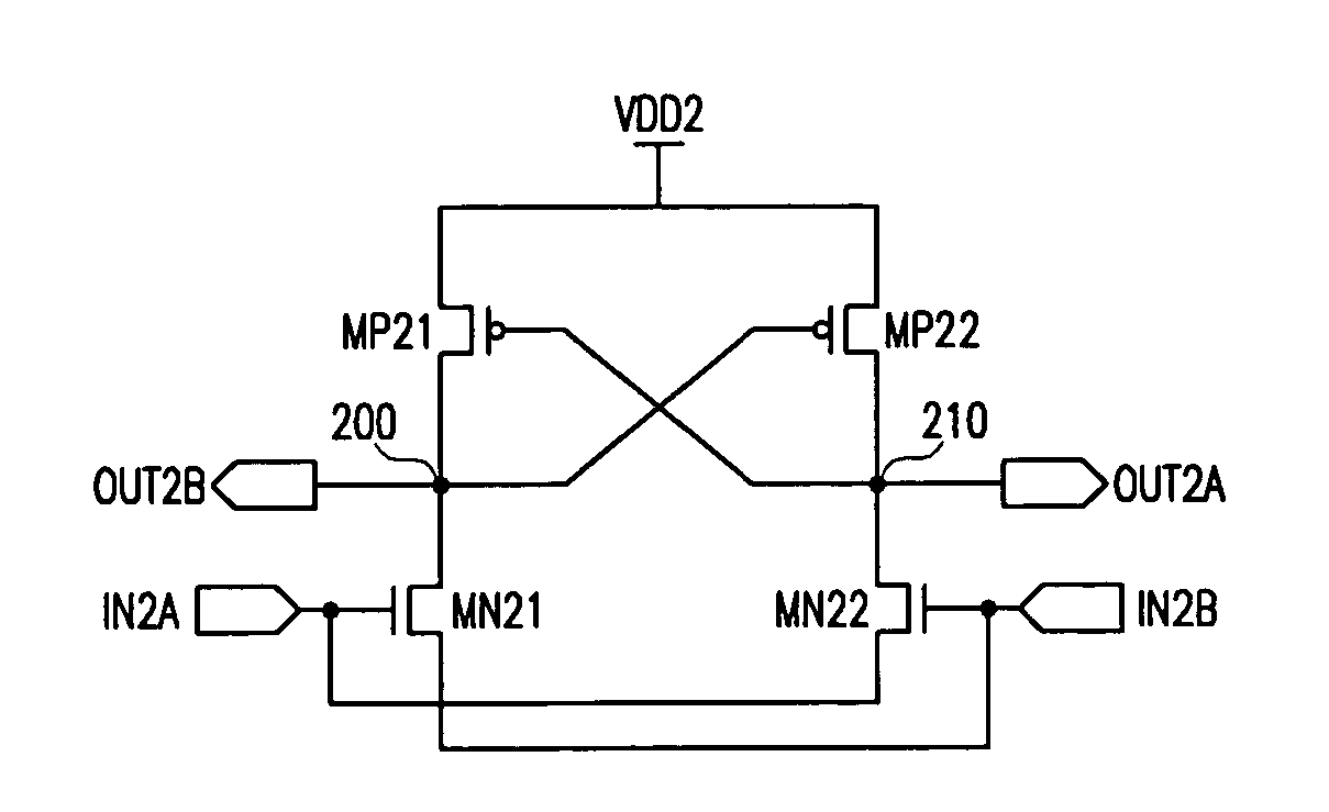
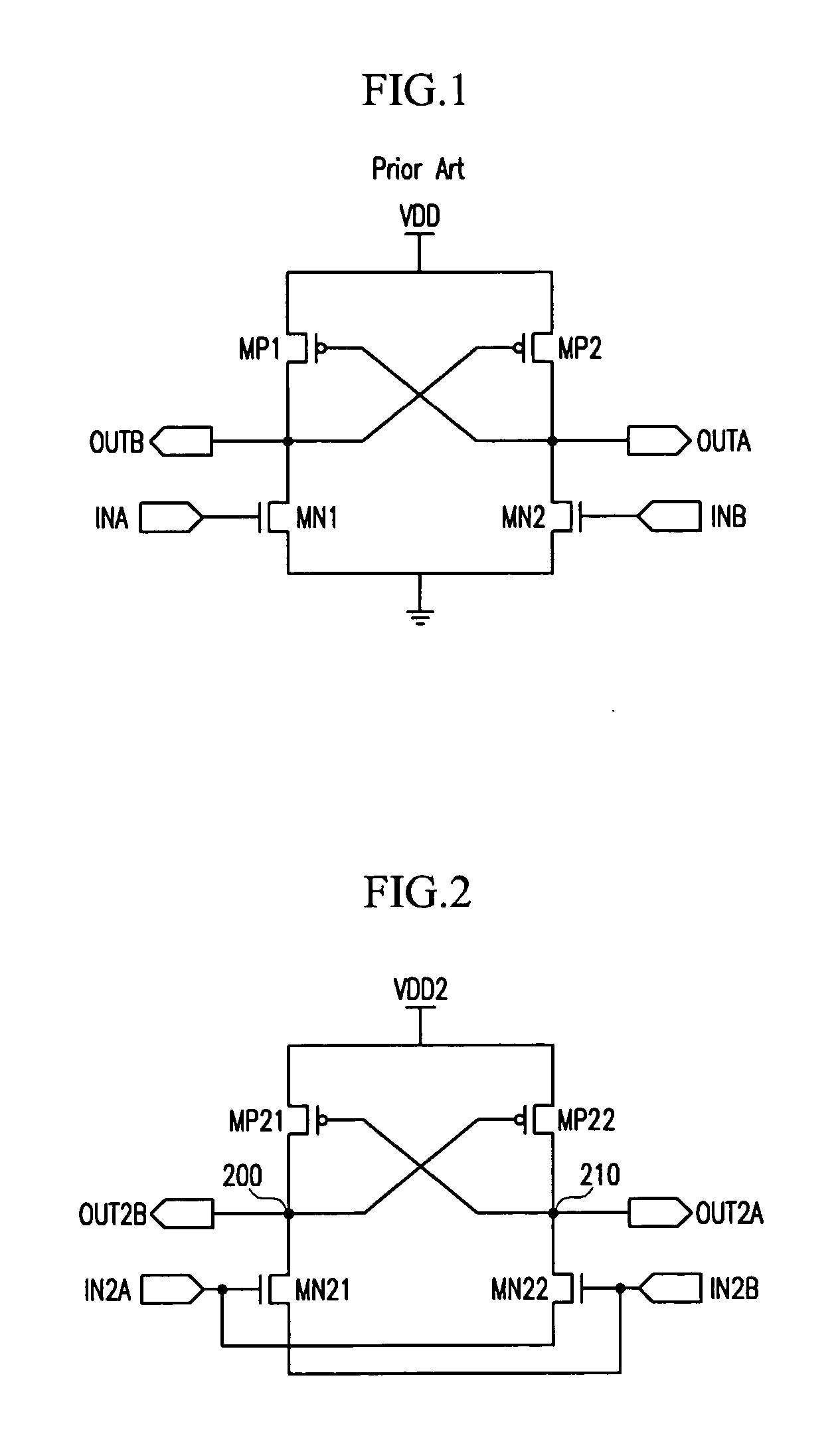
[0026]FIG. 2 shows a circuit diagram of a level shifter according to a first exemplary embodiment of the present invention.

[0027] As shown, the level shifter includes two PMOS transistors MP21 and MP22, two NMOS transistors MN21 and MN22, two output terminals OUT2A and OUT2B, and two input terminals IN2A and IN2B.

[0028] In detail, a drain of the transistor MP21 is coupled to a gate of the transistor MP22 and a first main electrode (a drain or a source) of the transistor MN21, and a drain of the transistor MP22 is coupled to a gate of...


PUM


Abstract

A level shifter includes first, second, third, and fourth transistors. The first transistor is operable by an applied first input signal and is for supplying a second input signal to a first main electrode of a transistor. The second transistor is operable by an applied second input signal and is for supplying a first input signal to a first main electrode of a transistor. The third transistor has a first main electrode coupled to a second main electrode of the first transistor and is operable by a signal outputted by the second transistor. The fourth transistor has a first main electrode coupled to a second main electrode of the second transistor and is operable by a signal outputted by the first transistor.

Description

CROSS REFERENCE TO RELATED APPLICATION [0001] This application claims priority to and the benefit of Korea Patent Application No. 10-2003-0085082 filed on Nov. 27, 2003 in the Korean Intellectual Property Office, the entire content of which is incorporated herein by reference. BACKGROUND OF THE INVENTION [0002] (a) Field of the Invention [0003] The present invention relates to a level shifter and a flat panel display. [0004] (b) Description of the Related Art [0005] A voltage level shifter is required in the design of a semiconductor integrated circuit (IC) so as to provide an interface between circuits which need different voltage levels. For example, an IC such as a DRAM operates within the range of a given voltage, but it may further require a signal voltage of greater than the range of a given voltage in order to interface with external circuits or provide signals to other circuits. [0006] The level shifter used for the above-described case is a circuit which is provided between...

Claims


Application Information

Patent Timeline
IPC IPC(8): G11C19/00G09G3/36H03K3/356
CPCG09G3/3674H03K3/356147H03K3/356113G09G2310/0289G11C19/00
Inventor PARK, YONG-SUNGKIM, YANG-WAN
Owner SAMSUNG SDI CO LTD
Why Eureka
Try Eureka